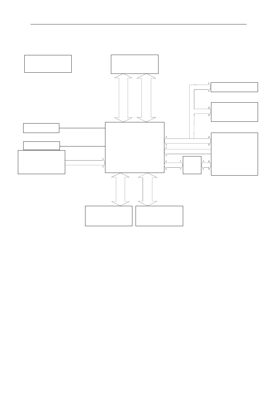
Block diagram, Architecture description, Block diagram architecture description – Sundance SMT376 User Manual
Page 7: Fpga controller

Version 1.7
Page 7 of 24
SMT376 User Manual
Block Diagram
83 I/O
2
x Comm-
Po
rt
s/
SDL
24
I/
O
p
ins
T
im
er,& C
ont
ro
l
15
I/
O
p
ins
2x Comm-
Po
rt/SDL
24
I/
O p
ins
G
lob
al
Bus
74
I/
O p
ins
JTAG Header
J1 Top Primary TIM
Connector
Comm-Port 0 & 3
J3 Global Expansion
Connector
J2 Bottom Primary TIM
Connector
Comm-Port 1 & 4
(2 linked with 5)
Linear regulators for
CPU & FPGA cores
Sundance High-speed Bus
(60-way Samtec)
Sundance Digital Bus
(40-way ODU)
4 LEDs &
4 I/O pins
256M bytes SDRAM (CE2,3)
8 x K4S560832
(32M x 8)
Flash (CE1)
Start-up mode selection.
64 pins
McBSP &
GPIO
Header
McBSP
'C6711/6713
DSP
FPGA Controller
Spartan-IIE, FG456
329 I/O Pins
XC2S300E
1.5V
TTL I/O
Architecture Description
The SMT376 TIM consists of a Texas Instruments TMS320C6211/6711/6713 running
at up to 225MHz. Modules are populated with 256MBytes of synchronous DRAM
(SDRAM).
A Field Programmable Gate Array (FPGA) is used to manage global bus accesses
and implement four communication ports and Sundance Digital/High-speed Buses.
This is a Xilinx Spartan –IIE device.