Chapter 3, Motherboard information – Lanner LEC-3110 User Manual
Page 14
12
Motherboard Information
Chapter 3
Embedded and Industrial Computing
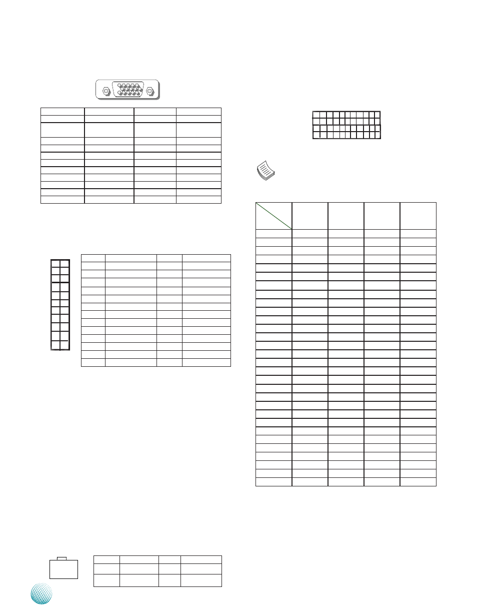
Pin No.
Description
Pin No.
Description
1
Red Color Signal
6
Ground
2
Green Color
Signal
7
Ground
3
Blue Color Signal
8
Ground
4
NC
9
VGA power
5
Ground
10
Ground
Pin No.
Description
11
NC
12
DDC-DATA
13
H-Sync.
14
V-Sync.
15
DDC-CLK
Front LED Connector (J2 ON LEB-3110): This is the
parallel connector for the front LED indicator Use the
26-pin connector to connect this port to the J1 connector
on LEK-LED01
SPI-ROM(J12): Using the appropriate cable to connect
this 10-pin ISP header connector, you can update the SPI
Flash soldered on board
LPC (LPC1) port (also called Port 80) (LPC1): It is a
proprietary connector for connecting a checkpoint device
to output checkpoints throughout booting and Power-
On Self Test (POST) to indicate the task the system is
currently executing.
SO-DIMM Socket (CN1): The SO-DIMM socket is used to
connect the DDR3 memory The system can support up to
2 GB in maximum
ATX Power Connector (ATX1): The main board is designed
to operate with a DC power input which is connected to
the DC/DC converter board The system has an AT-style
power input (VDC 24V) and system control
PCI-104 PCI Connector (J8 on LEB-3110): The
mainboard’s PCI-104 PCI expansion bus signals are
generated by the ICH8M
Note:
We recommend that you use only Lanner
1
I/O module with this connector to avoid
incompatibility as some pins have been altered
Row NO
Pin NO
Row A
Row B
Row C
Row D
1
KEY2
NC
VCC
AD0
2
VCC
AD2
AD1
VCC
3
AD5
GND
AD4
AD3
4
C/BE-0
AD7
GND
AD6
5
GND
AD9
AD8
GND
6
AD11
VCC
AD10
M66EN
7
AD14
AD13
GND
AD12
8
VCC3
C/BE-1
AD15
VCC3
9
SERR-
GND
SBO-
PAR
10
GND
PERR-
VCC3
SDONE
11
STOP-
VCC3
LOCK-
GND
12
VCC3
TRDY-
GND
DEVSEL-
13
FRAME-
GND
IRDY-
VCC3
14
GND
AD16
VCC3
C/BE-2
15
AD18
VCC3
AD17
GND
16
AD21
AD20
GND
AD19
17
VCC3
AD23
AD22
VCC3
18
IDSL0
GND
IDSL1
IDSL2
19
AD24
C/BE-3
VCC
IDSL3
20
GND
AD26
AD25
GND
21
AD29
VCC
AD28
AD27
22
VCC
AD30
GND
AD31
23
REQ-0
GND
REQ-1
VCC
24
GND
REQ-2
VCC
GNT-0
25
GNT-1
VCC
GNT-2
GND
26
VCC
PCICLK0
GND
PCICLK1
27
PCICLK2
VCC
PCICLK3
GND
28
GND
PIRQ-D
VCC
PCIRST-
29
+12V
PIRQ-A
PIRQ-B
PIRQ-C
30
-12V
NC
NC
KEY1
1
3
25
2
4
26
Pin No.
Function
Pin No.
Function
1
1 LAN1 LINK LED
2
LAN1 ACT LED
3
LAN2 LINK LED
4
LAN2 ACT LED
5
LAN3 LINK LED
6
LAN3 ACT LED
7
LAN4 LINK LED
8
LAN4 ACT LED
9
LAN5 LINK LED
10
LAN5 ACT LED
11
LAN6 LINK LED
12
LAN6 ACT LED
13
SW RESET
14
RUN LED
15
HW RESET
16
HDD LED
17
COM1 RX LED
18
COM2 RX LED
19
COM1 TX LED
20
COM2 TX LED
21
SIO GPIO60
22
SIO GPIO62
23
SIO GPIO61
24
SIO GPIO63
25
VCC3
26
GND
Pin No.
Function
Pin No.
Function
1
Ground
3
Ground
2
VCC12 (12V)
4
VCC12 (12V)
30 1
A
D
1
2
4
3
○
○
_
○
○
1
2
3
4
1
6
11
5
10
15