Board layout guidelines, Pad layout – Linx Technologies RXM-GPS-R4 User Manual
Page 16
–
–
–
–
26
27
Board Layout Guidelines
The module’s design makes integration straightforward; however, it
is still critical to exercise care in PCB layout. Failure to observe good
layout techniques can result in a significant degradation of the module’s
performance. A primary layout goal is to maintain a characteristic
50-ohm impedance throughout the path from the antenna to the module.
Grounding, filtering, decoupling, routing and PCB stack-up are also
important considerations for any RF design. The following section provides
some basic design guidelines which may be helpful.
During prototyping, the module should be soldered to a properly laid-out
circuit board. The use of prototyping or “perf” boards will result in poor
performance and is strongly discouraged.
The module should, as much as reasonably possible, be isolated from
other components on your PCB, especially high-frequency circuitry such as
crystal oscillators, switching power supplies, and high-speed bus lines.
When possible, separate RF and digital circuits into different PCB regions.
Make sure internal wiring is routed away from the module and antenna, and
is secured to prevent displacement.
Do not route PCB traces directly under the module. There should not be
any copper or traces under the module on the same layer as the module,
just bare PCB. The underside of the module has traces and vias that could
short or couple to traces on the product’s circuit board.
The Pad Layout section shows a typical PCB footprint for the module. A
ground plane (as large and uninterrupted as possible) should be placed on
a lower layer of your PC board opposite the module. This plane is essential
for creating a low impedance return for ground and consistent stripline
performance.
Use care in routing the RF trace between the module and the antenna or
connector. Keep the trace as short as possible. Do not pass under the
module or any other component. Do not route the antenna trace on
multiple PCB layers as vias will add inductance. Vias are acceptable for
tying together ground layers and component grounds and should be used
in multiples.
Each of the module’s ground pins should have short traces tying
immediately to the ground plane through a via.
Bypass caps should be low ESR ceramic types and located directly
adjacent to the pin they are serving.
A 50-ohm coax should be used for connection to an external antenna.
A 50-ohm transmission line, such as a microstrip, stripline or coplanar
waveguide should be used for routing RF on the PCB. The Microstrip
Details section provides additional information.
In some instances, a designer may wish to encapsulate or “pot” the
product. There is a wide variety of potting compounds with varying
dielectric properties. Since such compounds can considerably impact
RF performance and the ability to rework or service the product, it is
the responsibility of the designer to evaluate and qualify the impact and
suitability of such materials.
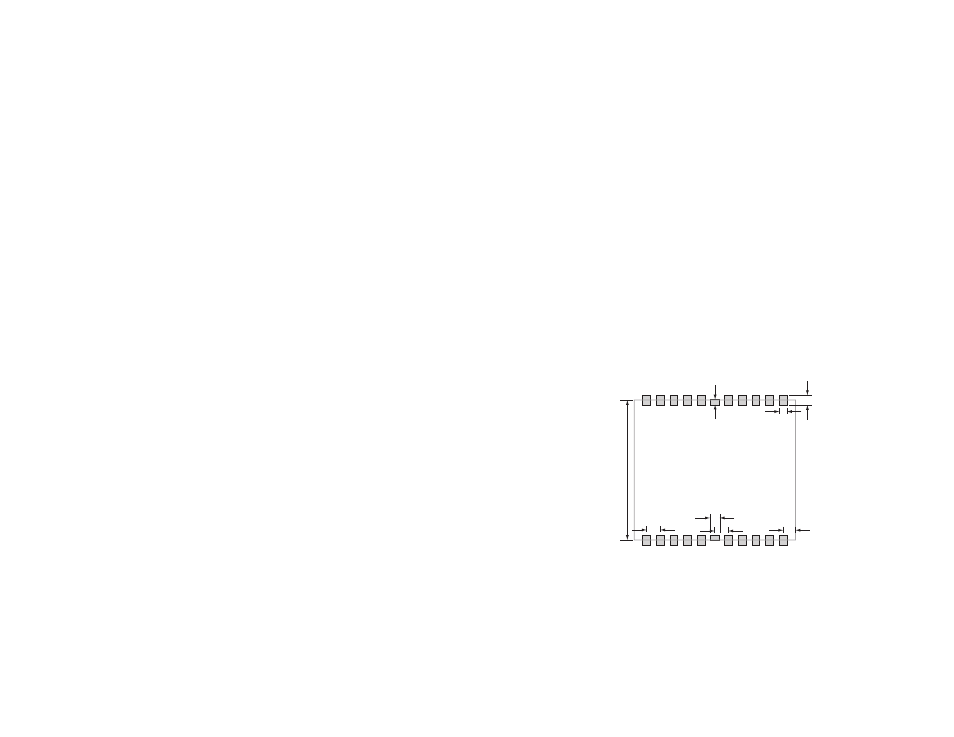
Pad Layout
The pad layout diagram in Figure 31 is designed to facilitate both hand and
automated assembly.
0.028
(0.70)
0.036
(0.92)
0.512
(13.00)
0.050
(1.27)
0.050
(1.27)
0.036
(0.92)
0.020
(0.50)
0.045
(1.15)
Figure 31: Recommended PCB Layout