Table 4.2 operating conditions, Operating conditions, Lvd driver scsi signals—sd[15:0 – Avago Technologies LSI53C320 User Manual
Page 44
4-2
Specifications
Version 2.2
Copyright © 2003 by LSI Logic Corporation. All rights reserved.
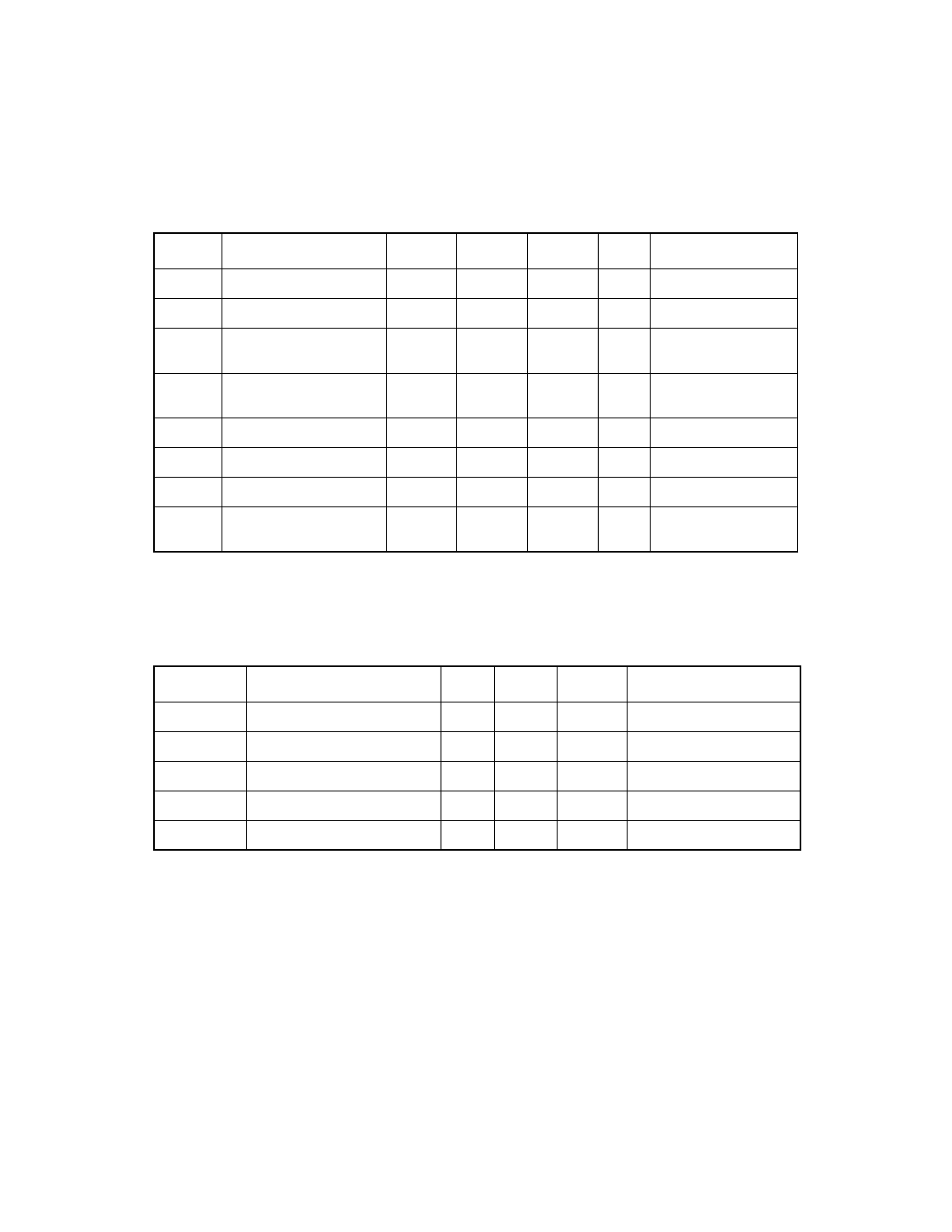
Table 4.2
Operating Conditions
1
Symbol
Parameter
Min
Nominal
Max
Unit
Test Conditions
V
DD-Core
Supply voltage
1.71
1.80
1.89
V
–
V
DD-IO
I/O Supply voltage
3.13
3.30
3.47
I
DD-Core
Core and Analog Supply
Current (Dynamic)
–
275
360
mA
–
I
DD-IO
I/O Supply Current
(Dynamic)
–
450
590
mA
RBIAS = 10 k
Ω
1%
V
DD
= 3.3 V
I
LP
2
Latch-up Current
150
–
–
mA
–
T
j
Junction Temperature
–
60
115
˚C
–
T
A
Operating free air
0
–
70
˚C
–
θ
JA
Thermal resistance
(junction to ambient air)
–
–
16.4
˚C/W
–
1. Conditions that exceed the operating limits can cause the device to function incorrectly.
2. SCSI pins only.
Table 4.3
LVD Driver SCSI Signals—SD[15:0]
±
, SDP[1:0]
±
, SCD
±
, SIO
±
, SMSG
±
,
SREQ
±
, SACK
±
, SBSY
±
, SATN
±
, SSEL
±
, SRST
±
1
Symbol
Parameter
Min
Max
Units
Test Conditions
I
O
+
Source (+) current
9.6
14.4
mA
Asserted state
I
O
−
Sink (
−
) current
−
9.6
−
14.4
mA
Asserted state
I
O
+
Source (+) current
−
6.4
−
9.6
mA
Negated state
I
O
−
Sink (
−
) current
6.4
9.6
mA
Negated state
I
OZ
3-state leakage
−
20
20
µ
A
–
1. V
CM
= 0.7
−
1.8 V, R
bias
= 10 k
Ω.