Tolerant technology electrical characteristics – Avago Technologies LSI53C825AE User Manual
Page 236
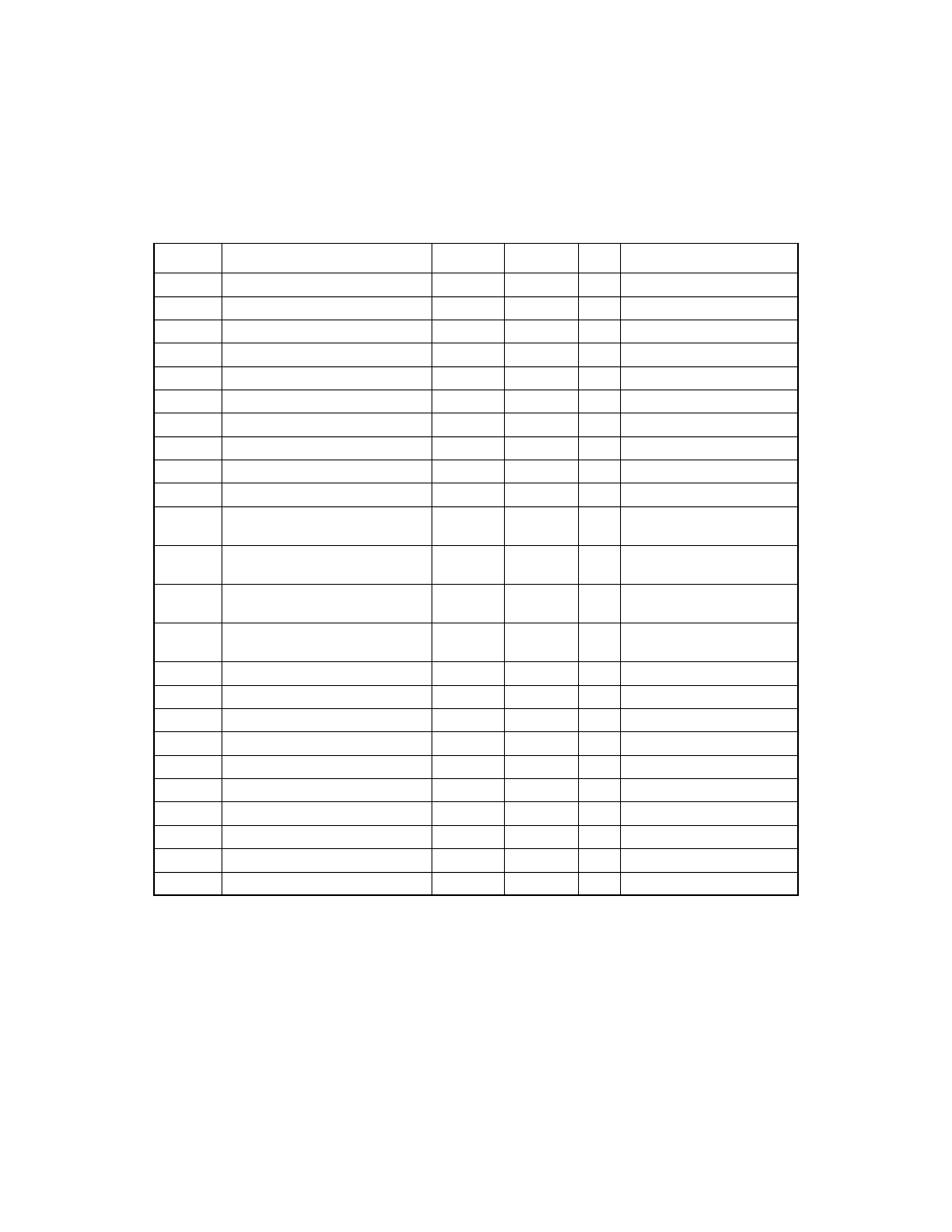
6-8
Specifications
Table 6.15
TolerANT Technology Electrical Characteristics
Symbol
Parameter
Min
Max
Unit
Test Conditions
V
OH
1
1. Active negation outputs only: Data, Parity, SREQ/, SACK/.
Output high voltage
2.5
3.5
V
I
OH
= 2.5 mA
V
OL
Output low voltage
0.1
0.5
V
I
OL
= 48 mA
V
IH
Input high voltage
2.0
7.0
V
–
V
IL
Input low voltage
−
0.5
0.8
V
Referenced to V
SS
V
IK
Input clamp voltage
−
0.66
−
0.77
V
V
DD
= 4.75; I
I
=
−
20 mA
V
TH
Threshold, HIGH to LOW
1.1
1.3
V
–
V
TL
Threshold, LOW to HIGH
1.5
1.7
V
–
V
TH
–V
TL
Hysteresis
200
400
mV
–
I
OH
1
Output high current
2.5
24
mA
V
OH
= 2.5 V
I
OL
Output low current
100
200
mA
V
OL
= 0.5 V
I
OSH
1
Short-circuit output high current
–
625
mA
Output driving low, pin
shorted to V
DD
supply
2
2. Single pin only; irreversible damage may occur if sustained for one second.
I
OSL
Short-circuit output low current
–
95
mA
Output driving high, pin
shorted to V
SS
supply
I
LH
Input high leakage
–
10
µ
A
−
0.5 < V
DD
< 5.25
V
PIN
= 2.7 V
I
LL
Input low leakage
–
−
10
µ
A
−
0.5 < V
DD
< 5.25
V
PIN
= 0.5 V
R
I
Input resistance
20
–
M
Ω
SCSI pins
3
3. SCSI RESET pin has 10 k
Ω
pull-up resistor.
Note: These values are guaranteed by periodic characterization; they are not 100% tested on every
device.
C
P
Capacitance per pin
–
10
pF
PQFP
t
R
1
Rise time, 10% to 90%
9.7
18.5
ns
t
F
Fall time, 90% to 10%
5.2
14.7
ns
dV
H
/dt
Slew rate, LOW to HIGH
0.15
0.49
V/ns
dV
L
/dt
Slew rate, HIGH to LOW
0.19
0.67
V/ns
ESD
Electrostatic discharge
2
–
kV
MIL-STD-883C; 3015-7
Latch-up
100
–
mA
–
Filter delay
20
30
ns
Extended filter delay
40
60
ns