Fairchild SEMICONDUCTOR RC5051 User Manual
Page 3
APPLICATION NOTE
AN50
3
I/O Controls
In addition to the Voltage Identification, there are several sig-
nals that control the DC-DC converter or provide feedback
from the DC-DC converter to the CPU. They are Power-
Good (PWRGD), Output Enable (OUTEN), and Upgrade
Present (UP#). These signals will be discussed later.
RC5050 and RC5051 Description
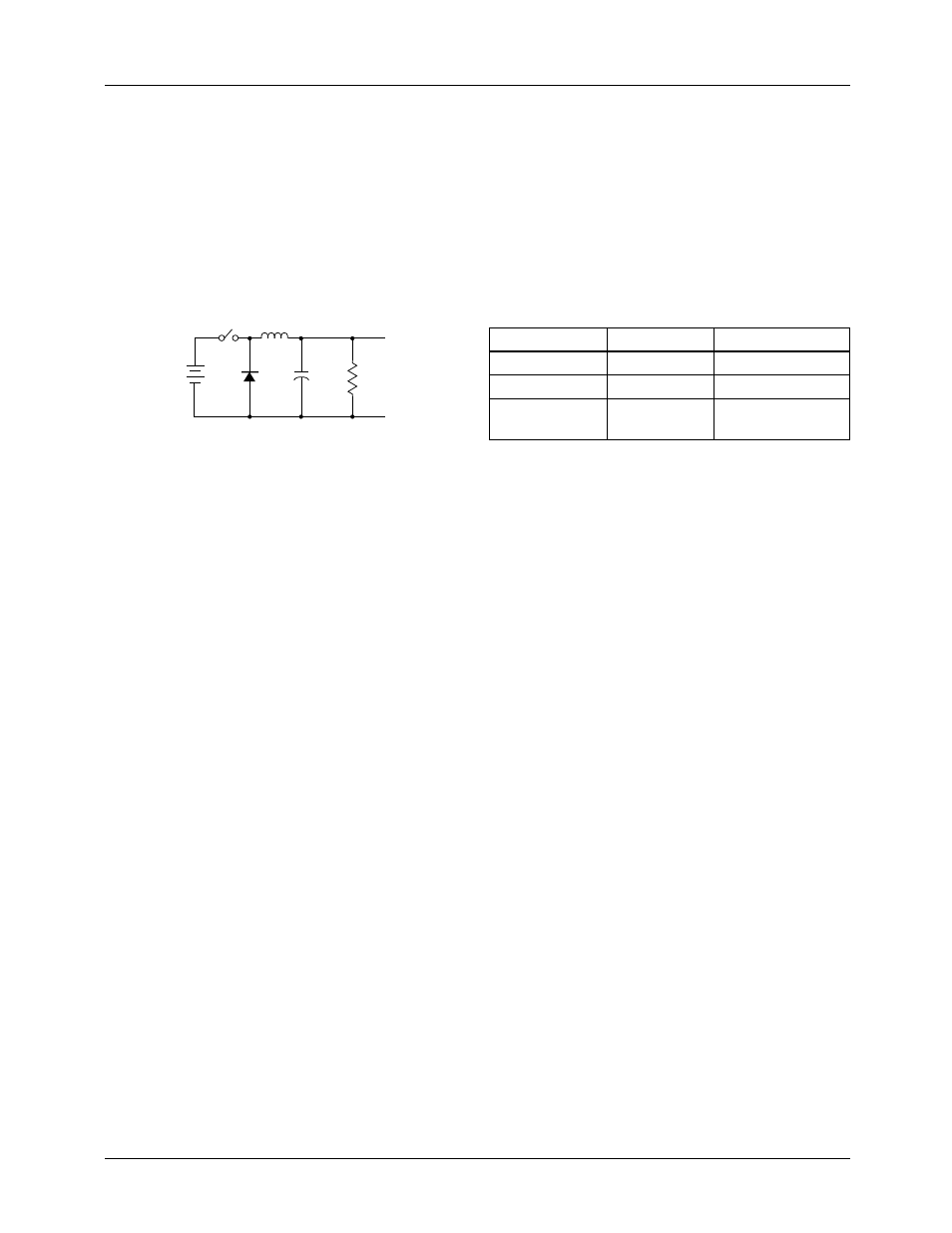
Simple Step-Down Converter
Figure 1. Simple Buck DC-DC Converter
Figure 1 illustrates a step-down DC-DC converter with no
feedback control. The derivation of the basic step-down con-
verter is the basis for the design equations for the RC5050
and RC5051. Referring to Figure 1, the basic operation
begins by closing the switch S1. When S1 is closed, the input
voltage V
IN
is impressed across inductor L1. The current
flowing in this inductor is given by the following equation:
where T
ON
is the duty cycle (the time when S1 is closed).
When S1 opens, the diode D1 conducts the inductor
current and the output current is delivered to the load accord-
ing to the following equation:
whereT
S
is the overall switching period and (T
S
- T
ON
) is the
time during which S1 is open.
By solving these two equations, we can arrive at the basic
relationship for the output voltage of a step-down converter:
In order to obtain a more accurate approximation for V
OUT
,
we must also include the forward voltage V
D
across diode
D1 and the switching loss, V
SW
. After taking into account
these factors, the new relationship becomes:
where V
SW
= MOSFET switching loss
= I
L
• R
DS,ON
The RC5050 and RC5051 Controllers
The RC5050 is a programmable non-synchronous DC-DC
controller IC. The RC5051 is a synchronous version of the
RC5050. When designed around the appropriate external
components, either of these devices can be configured to
deliver more than 14.5A of output current. The RC5050 and
RC5051 utilize both current-mode and voltage-mode PWM
control to create an integrated step-down voltage regulator.
The key differences between the RC5050 and RC5051 are
listed in Table 4.
Table 4. RC5050 and RC5051 Differences
Main Control Loop
Refer to the RC5051 Block Diagram illustrated in Figure 2.
The control loop of the regulator contains two main sections;
the analog control block and the digital control block. The
analog section consists of signal conditioning amplifiers
feeding into a set of comparators which provide the inputs to
the digital control block. The signal conditioning section
accepts inputs from the IFB (current feedback) and VFB
(voltage feedback) pins and sets up two controlling signal
paths. The voltage control path amplifies the VFB signal and
presents the output to one of the summing amplifier inputs.
The current control path takes the difference between the
IFB and VFB pins and presents the resulting signal to
another input of the summing amplifier. These two signals
are then summed together with the slope compensation input
from the oscillator. This output is then presented to a
comparator, which provides the main PWM control signal to
the digital control block.
The additional comparators in the analog control section set
the point at which the current limit comparator disables the
output drive signals to the external power MOSFETs.
The digital control block takes the comparator inputs and the
main clock signal from the oscillator to provide the appropri-
ate pulses to the HIDRV and LODRV output pins. These
pins control the external power MOSFETs. The digital sec-
tion utilizes high speed Schottky transistor logic, allowing
the RC5050 and the RC5051 to operate at clock speeds as
high as 1MHz.
High Current Output Drivers
The RC5051 contains two identical high current output
drivers that utilize high speed bipolar transistors in a
push-pull configuration. Each driver is capable of
delivering 1A of current in less than 100ns. Each driver’s
power and ground are separated from the chip’s power and
ground for additional switching noise immunity.
C1
R
L
Vout
+
–
D1
V
IN
65-5050-06
L1
S1
I
L
V
IN
V
OUT
–
(
)
T
ON
L1
-----------------------------------------------
=
I
L
V
OUT
T
S
T
ON
–
(
)
L1
-------------------------------------------
=
V
OUT
V
IN
T
ON
T
S
-----------
=
V
OUT
V
IN
V
D
V
SW
–
+
(
)
T
ON
T
S
-----------
V
D
–
=
RC5051
RC5050
Operation
Synchronous
Non-Synchronous
Package
20-SOIC
20-SOIC
Output Enable/
Disable
Yes
Yes