Maximum ratings, Thermal characteristics, Electrical characteristics – Diodes DMN62D1SFB User Manual
Page 2
DMN62D1SFB
Document number: DS35252 Rev. 3 - 2
2 of 6
April 2014
© Diodes Incorporated
ADVAN
CE I
N
F
O
RM
ATI
O
N
DMN62D1SFB
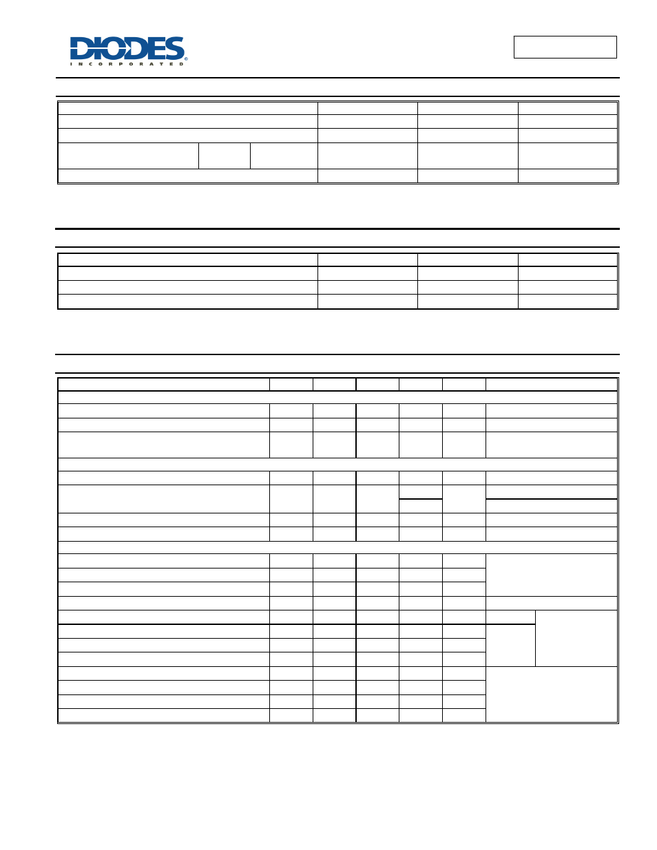
Maximum Ratings
(@T
A
= +25°C, unless otherwise specified.)
Characteristic
Symbol
Value
Unit
Drain-Source Voltage
V
DSS
60 V
Gate-Source Voltage
V
GSS
±20 V
Continuous Drain Current (Note 5) V
GS
= 10V
T
A
= +25°C
T
A
= +85°C
I
D
0.41
0.30
A
Pulsed Drain Current (Note 6)
I
DM
2.64 A
Thermal Characteristics
(@T
A
= +25°C, unless otherwise specified.)
Characteristic Symbol
Value
Unit
Power Dissipation (Note 5)
P
D
0.47 W
Thermal Resistance, Junction to Ambient @T
A
=+25°C R
θJA
258 °C/W
Operating and Storage Temperature Range
T
J
,
T
STG
-55 to +150
°C
Electrical Characteristics
(@T
A
= +25°C, unless otherwise specified.)
Characteristic
Symbol
Min
Typ
Max
Unit
Test Condition
OFF CHARACTERISTICS (Note 7)
Drain-Source Breakdown Voltage
BV
DSS
60 — — V
V
GS
= 0V, I
D
= 250μA
Zero Gate Voltage Drain Current T
J
= +25°C
I
DSS
— — 100 nA
V
DS
= 60V, V
GS
= 0V
Gate-Source Leakage
I
GSS
— —
10
1
μA
V
GS
= ±20V, V
DS
= 0V
V
GS
= ±5V, V
DS
= 0V
ON CHARACTERISTICS (Note 7)
Gate Threshold Voltage
V
GS(th)
1.3 1.6 2.3 V
V
DS
= V
GS
, I
D
= 250μA
Static Drain-Source On-Resistance
R
DS(ON)
— —
1.40
Ω
V
GS
= 10V, I
D
= 40mA
1.60
V
GS
= 4.5V, I
D
= 35mA
Forward Transfer Admittance
|Y
fs
|
100
— — mS
V
DS
= 5V, I
D
= 40mA
Diode Forward Voltage
V
SD
— 0.7 1.1 V
V
GS
= 0V, I
S
= 300mA
DYNAMIC CHARACTERISTICS (Note 8)
Input Capacitance
C
iss
— 40 80 pF
V
DS
= 40V, V
GS
= 0V,
f = 1.0MHz
Output Capacitance
C
oss
— 3.5 7 pF
Reverse Transfer Capacitance
C
rss
— 2.8 5.6 pF
Gate Resistance
R
g
— 81.3 200 Ω
V
DS
= 0V, V
GS
= 0V, f = 1MHz
Total Gate Charge
Q
g
— 0.73 1.5 nC
V
GS
= 4.5V
V
DS
= 50V, I
D
= 1A
Total Gate Charge
Q
g
— 1.39 2.8 nC
V
GS
= 10V
Gate-Source Charge
Q
gs
— 0.2 0.4 nC
Gate-Drain Charge
Q
gd
— 0.23 0.5 nC
Turn-On Delay Time
t
D(on)
— 3.89 10 ns
V
DS
= 50V, I
D
= 1A
V
GS
= 10V, R
G
= 6Ω
Turn-On Rise Time
t
r
— 4.93 10 ns
Turn-Off Delay Time
t
D(off)
— 18.80 40 ns
Turn-Off Fall Time
t
f
— 11.96 25 ns
Notes:
5. Device mounted on FR-4 PCB, with minimum recommended pad layout.
6. Device mounted on minimum recommended pad layout test board, 10µs pulse duty cycle = 1%.
7. Short duration pulse test used to minimize self-heating effect.
8. Guaranteed by design. Not subject to production testing.