Altera 100G Development Kit, Stratix V GX Edition User Manual
Page 16
4–4
Chapter 4: Development Board Setup
Factory Default Switch Settings
100G Development Kit, Stratix V GX Edition
August 2012
Altera Corporation
User Guide
3. Set jumper blocks (J9, J62) to match
and
f
For more information about the FPGA board settings, refer to the
5
REFCLKB_SEL
Switch 5 has the following options:
■
When on (1), the SMA is selected.
■
When off (0), the PLL is selected.
0
6
CLK_644_EN
Switch 6 has the following options:
■
When on (1), 644-MHz clock is enabled.
■
When off (10, 644-MHz clock is disabled.
1
7
SECURITY
Switch 7 has the following options:
■
When on (1), configuration security is enabled.
■
When off (0), configuration security is disabled.
When enabled, the FPGA cannot be accessed via JTAG if the device has
already been programmed by the PFL.
1
8
—
—
—
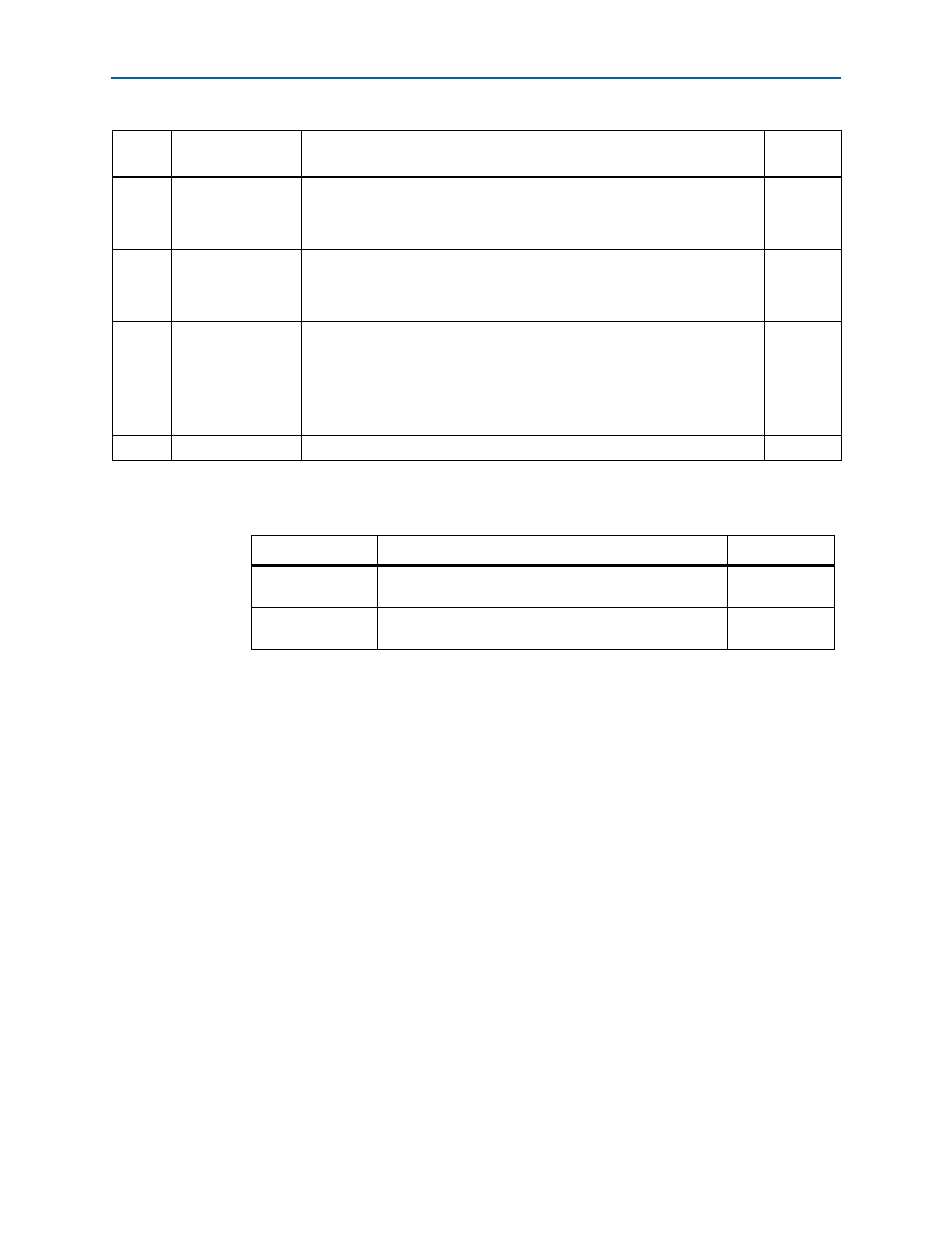
Table 4–2. SW3 DIP Switch Settings (Part 2 of 2)
Switch
Board
Label
Function
Default
Position
Table 4–3. Jumper Settings
Board Reference
Description
Shunt Position
J9
Fan Bypass — Shut installed forces the fan to ON and at
full speed.
Not Installed
J62
MAX_JTAG_EN (logic 1) — Shunt installed removes
MAX II from JTAG chain.
Not Installed