Configuration space register access timing – Altera Stratix V Avalon-MM Interface for PCIe Solutions User Manual
Page 59
Bit(s)
Field
Description
[6:4]
multiple message
enable
This field indicates permitted values for MSI signals. For example,
if “100” is written to this field 16 MSI signals are allocated.
• 3’b000: 1 MSI allocated
• 3’b001: 2 MSI allocated
• 3’b010: 4 MSI allocated
• 3’b011: 8 MSI allocated
• 3’b100: 16 MSI allocated
• 3’b101: 32 MSI allocated
• 3’b110: Reserved
• 3’b111: Reserved
[3:1]
multiple message
capable
This field is read by system software to determine the number of
requested MSI messages.
• 3’b000: 1 MSI requested
• 3’b001: 2 MSI requested
• 3’b010: 4 MSI requested
• 3’b011: 8 MSI requested
• 3’b100: 16 MSI requested
• 3’b101: 32 MSI requested
• 3’b110: Reserved
[0]
MSI Enable
If set to 0, this component is not permitted to use MSI.
Related Information
•
•
Configuration Space Register Access Timing
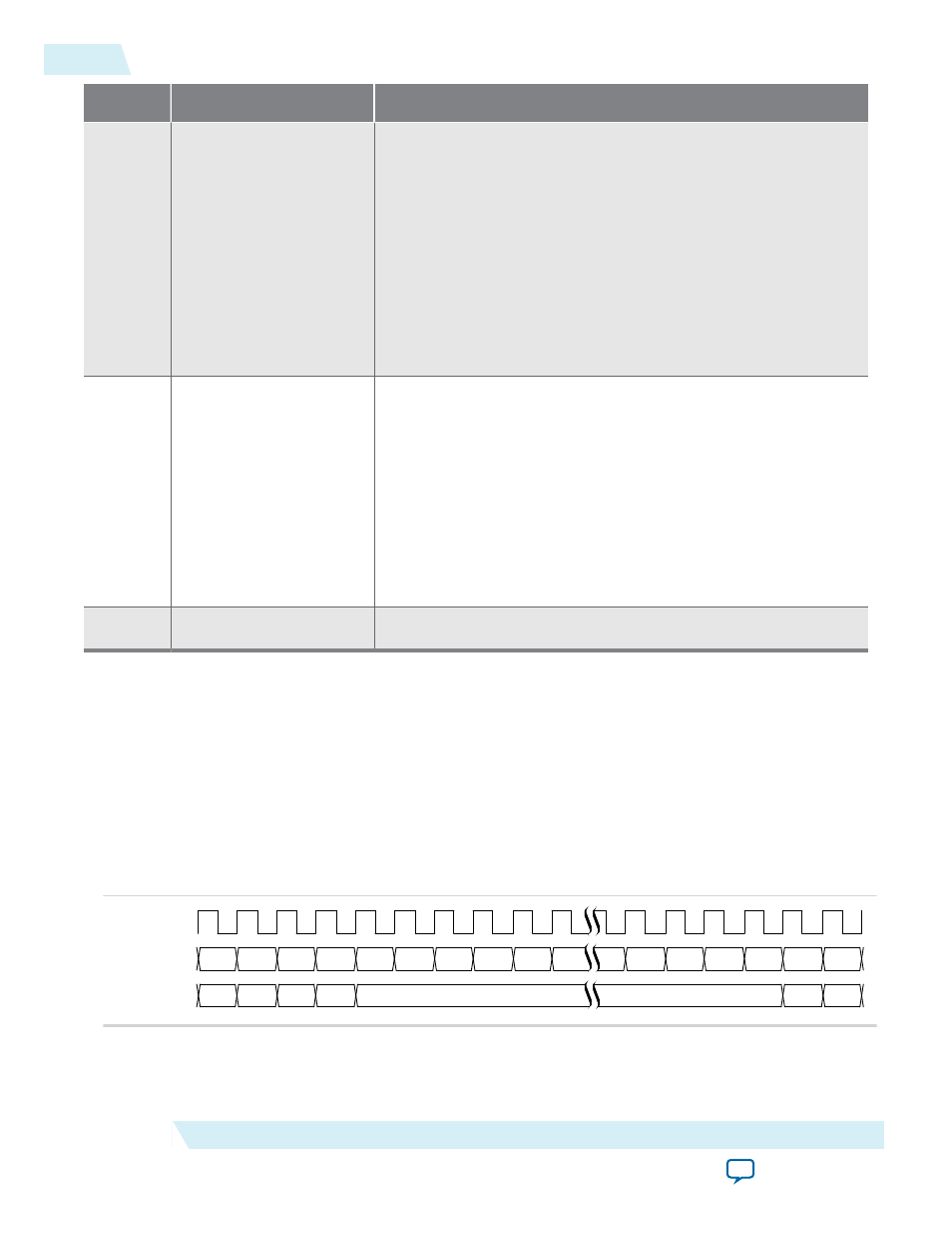
Figure 4-8: tl_cfg_ctl Timing
The following figure shows typical traffic on the
tl_cfg_ctl
bus. The
tl_cfg_add
index increments on
the rising edge of the
pld_clk
. The address specifies which Configuration Space register data value is
being driven onto
tl_cfg_ctl
.
pld_clk
tl_cfg_add[3:0]
tl_cfg_ctl[31:0]
2
3
4
5
6
7
8
9
A
B
8
9
A
B
C
D
E
00... 00... 00... 7F...
00000000
00000000
00... 00...
4-26
Configuration Space Register Access Timing
UG-01097_avmm
2014.12.15
Altera Corporation
64- or 128-Bit Avalon-MM Interface to the Application Layer