Max v cpld system controller, Max v cpld system controller –6 – Altera Stratix V GX FPGA Development Board User Manual
Page 14
2–6
Chapter 2: Board Components
MAX V CPLD System Controller
Stratix V GX FPGA Development Board
October 2014
Altera Corporation
Reference Manual
MAX V CPLD System Controller
The board utilizes the 5M2210ZF256C4 System Controller, an Altera MAX V CPLD,
for the following purposes:
■
FPGA configuration from flash memory
■
Power consumption monitoring
■
Temperature monitoring
■
Fan control
■
Control registers for clocks
■
Control registers for remote system update
Flash
1.8-V CMOS
68
—
PCI Express ×8
2.5-V CMOS + XCVR
43
1 REFCLK
HSMC Port A
2.5-V CMOS + LVDS + XCVR
118
1 REFCLK
HSMC Port B
2.5-V CMOS + DQS + XCVR
104
1 REFCLK
Gigabit Ethernet
2.5-V CMOS + LVDS
8
—
On-Board USB-Blaster II
1.5-V CMOS
18
—
3.3-V CMOS
1
—
SDI Video
2.5-V CMOS + XCVR
8
1 REFCLK
QSFP
2.5-V CMOS + XCVR
23
1 REFCLK
Buttons
1.8/2.5-V CMOS
4
1 DEV_CLRn
Switches
1.8-V CMOS
8
—
Character LCD
2.5-V CMOS
11
—
LEDs
1.8/2.5-V CMOS
16
—
Clocks or Oscillators
1.8-V CMOS + LVDS
25
9 REFCLK
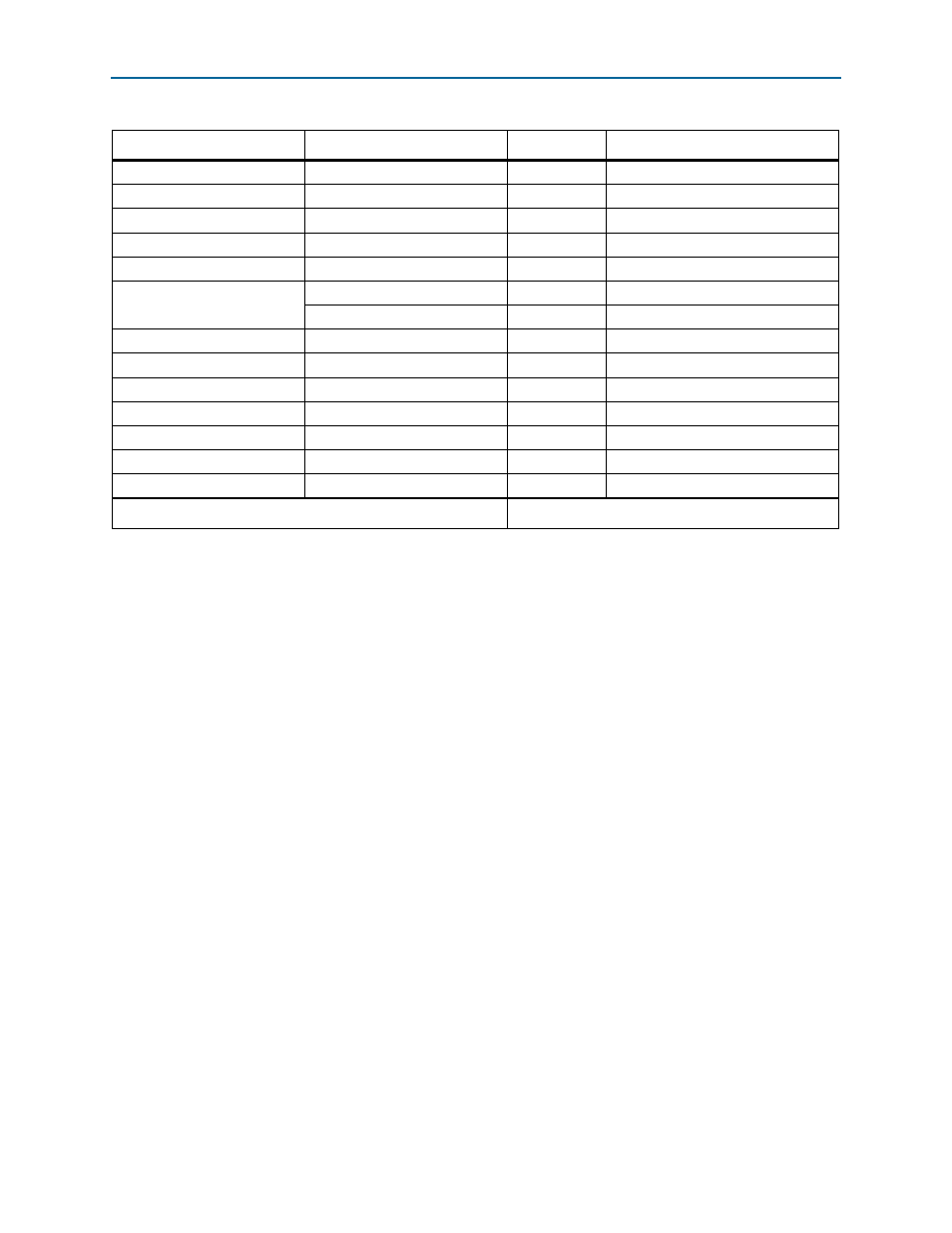
Device I/O Total:
713
Table 2–4. Stratix V GX FPGA Pin Count and Usage (Part 2 of 2)
Function
I/O Standard
I/O Count
Special Pins