Qdr ii interface, Qdr ii interface –55 – Altera 100G Development Kit, Stratix V GX Edition User Manual
Page 63
Chapter 2: Board Components
2–55
Components and Interfaces
August 2012
Altera Corporation
100G Development Kit, Stratix V GX Edition
Reference Manual
lists the DDR3 interfaces component reference and manufacturing
information.
QDR II Interface
The QDR II interface consists of two 72-Mbit QDR II burst-of-two SRAM devices.
Port A has a 18-bit read data bus and a 18-bit write data bus while Port B has 36-bit
busses. The target speed is 300 MHz with a theoretical bandwidth of 10.8 Gbps for
Port A and 21.6 Gbps for Port B (total bandwidth of 32.4 Gbps or 64.8 Gbps for
simultaneous read and write).
lists the pin assignments for the QDR II interface and their corresponding
schematic signal names and Stratix V GX pin numbers.
A2
DDR3F_DQ29
1.5-V SSTL
L32
Data bus
B8
DDR3F_DQ30
1.5-V SSTL
P34
Data bus
A3
DDR3F_DQ31
1.5-V SSTL
L33
Data bus
F3
DDR3F_DQS_P0
1.5-V SSTL
C34
Data strobe P byte lane 0
G3
DDR3F_DQS_N0
1.5-V SSTL
B34
Data strobe N byte lane 0
C7
DDR3F_DQS_P1
1.5-V SSTL
T33
Data strobe P byte lane 1
B7
DDR3F_DQS_N1
1.5-V SSTL
T32
Data strobe N byte lane 1
F3
DDR3F_DQS_P2
1.5-V SSTL
H35
Data strobe P byte lane 2
G3
DDR3F_DQS_N2
1.5-V SSTL
G35
Data strobe N byte lane 2
C7
DDR3F_DQS_P3
1.5-V SSTL
U35
Data strobe P byte lane 3
B7
DDR3F_DQS_N3
1.5-V SSTL
T35
Data strobe N byte lane 3
K1
DDR3F_ODT
1.5-V SSTL
B37
On-die termination
J3
DDR3F_RASN
1.5-V SSTL
K34
Row address select
T2
DDR3F_RSTN
1.5-V SSTL
N38
Reset
L3
DDR3F_WEN
1.5-V SSTL
V36
Write enable
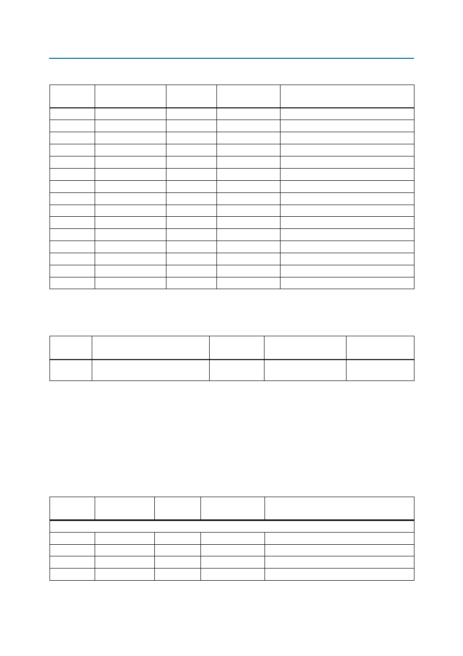
Table 2–35. DDR3 Interface Pin Assignments, Schematic Signal Names, and Functions (Part 11 of 11)
Board
Reference
Schematic Signal
Name
I/O Standard
Stratix V GX
Device Pin Number
Description
Table 2–36. DDR3 interfaces Component Reference And Manufacturing Information
Board
Reference
Description
Manufacturer
Manufacturing
Part Number
Manufacturer
Website
U24-U29,
U31-U36
16 M × 16-bit × 8 banks, 667M, CL9
DDR3 device
Micron
MT41J128M16HA-125
Table 2–37. QDR II Interface Pin Assignments, Schematic Signal Names, and Functions (Part 1 of 6)
Board
Reference
Schematic Signal
Name
I/O Standard
Stratix V GX
Device Pin Number
Description
QDRII Port A Interface (U41)
R9
QDR2A_A0
1.5-V HSTL
AP24
Address bus
R8
QDR2A_A1
1.5-V HSTL
AL24
Address bus
B4
QDR2A_A2
1.5-V HSTL
AR23
Address bus
B8
QDR2A_A3
1.5-V HSTL
BB26
Address bus