Altera Nios Development Board Stratix II Edition User Manual
Page 53
Altera Corporation
Reference Manual
2–43
May 2007
Nios Development Board Stratix II Edition
Board Components
The FPGA receives clock input from buffer U2, and from the PROTO1 and
PROTO2 connectors, as shown in
The FPGA can synthesize new clock signals internally using on-chip
PLLs, and drive the clocks to various components on the board, as shown
in
The 50 MHz oscillator (Y2) is socketed and can be changed or removed by
the user. To drive the clock circuitry using the external clock connector
(J4), remove Y2.
1
The factory-programmed configuration controller and Altera-
provided reference designs work only with the 50 MHz clock.
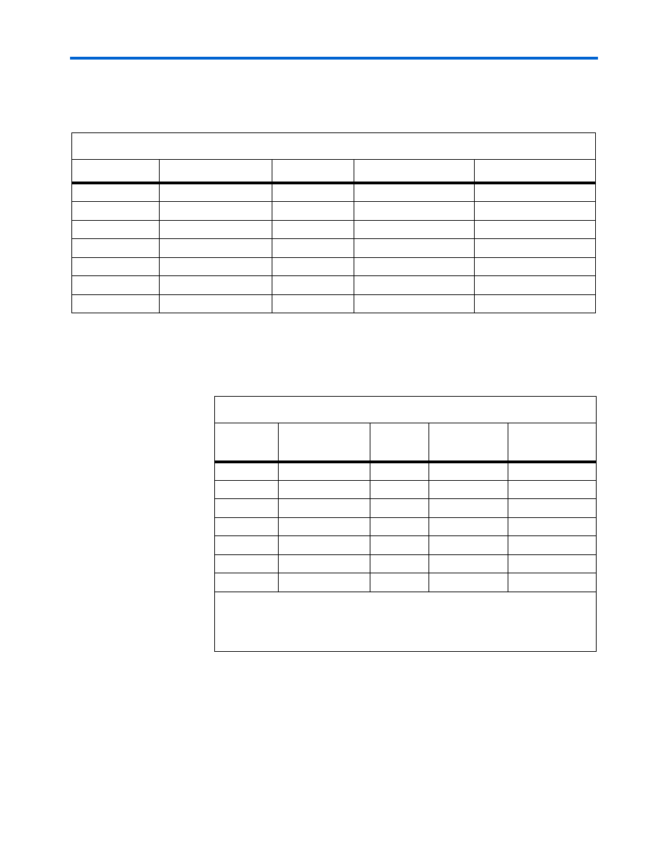
Table 2–21. FPGA Clock Input Pin Table
FPGA Pin
FPGA Pin Name
PLL
Signal Source
Board Net Name
R1
CLK8p
PLL3, PLL4
J25 pin 6
mictor_TRCLK
R26
CLK2p
PLL1, PLL2
J13 pin 13
proto1_CLKOUT
P2
CLK10p
PLL3, PLL4
J17 pin 13
proto2_CLKOUT
B13
CLK12p
PLL5
U2 pin 2
osc_CLK0
P25
CLK0p
PLL1, PLL2
U2 pin 3
osc_CLK1
AC13
CLK7p
PLL6
U2 pin 4
osc_CLK2
R3
CLK9p
PLL3, PLL4
U2 pin 6
osc_CLK3
Table 2–22. FPGA Clock Output Pin Table
FPGA Pin
FPGA Pin Name
PLL
Signal
Destination
Board Net Name
C3
IO
N/A
U63 pin 45
sdram_CLK_p
C4
IO
N/A
U63 pin 46
sdram_CLK_n
A12
PLL5_OUT0p
PLL5
(1)
U74 pin 89
sram_CLK
AE14
IO
N/A
JH1 pin 13
pmc_CLK
K6
IO
N/A
J13 pin 11
proto1_PLLCLK
K7
IO
N/A
J17 pin 11
proto2_PLLCLK
AD15
PLL12_OUT0p
PLL12
(1)
J25 pin 5
mictor_CLK
Note to
(1)
PLLS pins are only dedicated when using the Enhanced PLL. If you use the Fast
PLL, the PLL inputs and outputs can be routed to any user pin on the device. For
more information on using PLLs in the Stratix II refer to the data sheet.