Register bit definitions – NEXCOM NSA 3150 User Manual
Page 70
Copyright © 2013 NEXCOM International Co., Ltd. All Rights Reserved.
56
NSA 3150 User Manual
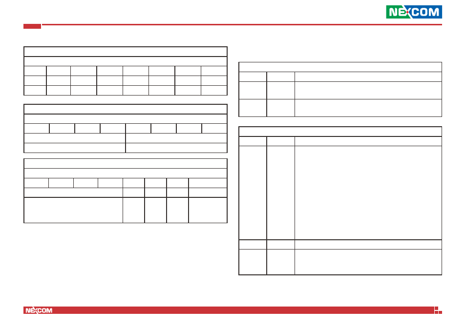
Appendix A: Bypass Register
Slot Select Register
Offset 0xF9
7
6
5
4
3
2
1
0
R/W
R/W
R/W
R/W
R/W
R/W
R/W
R/W
Slot ID 7
Slot ID 6
Slot ID 5
Slot ID 4
Slot ID 3
Slot ID 2
Slot ID 1
Slot ID 0
PCB and CPLD Release Version Register (MSB)
Offset 0xFD
7
6
5
4
3
2
1
0
R
R
PCB version (MSB) / CPLD dot version
CPLD release version (MSB)
Bypass Time/Force Mode Control Register
Offset 0xFE
7
6
5
4
3
2
1
0
R
R/W
R/W
R/W
R/W
CPLD identify bit
Unused Unused
Unused
Timer/
force mode
independent
Bypass Timer Configuration Register: F2
Bit Field
Name
Value
2:0
Timer
Value
000 = 0 second, timer immediately expired
001 = 1 second
010 = 2 second
011 = 4 second
100 = 8 second
101 = 16 second
110 = 32 second
111 = 64 second
This register is available in Timer Enable mode. Timer value of 1 to
7 is required to be written before expiration of the hardware timer.
When the timer expires, both segment relays which have been
enabled will close.
Note: The timer will recount while read/write F2 register.
6:3
Unused
Unused
7
Segment
Timer
Expired
Read only bit:
0 = Timer has not expired
1 = Timer has expired, de-assert while leave Timer mode
PCB and CPLD Release Version Register (LSB): F1
Bit Field
Name
Value
3:0
CPLD
version LSB
CPLD version LSB, for CPLD release version control, the MSB info at
address ‘FD’, Read only
7:4
PCB
version LSB
PCB version LSB, the MSB info at address ‘FD’, Read only
Register Bit Definitions