NEXCOM NSA 3150 User Manual
Page 71
Copyright © 2013 NEXCOM International Co., Ltd. All Rights Reserved.
57
NSA 3150 User Manual
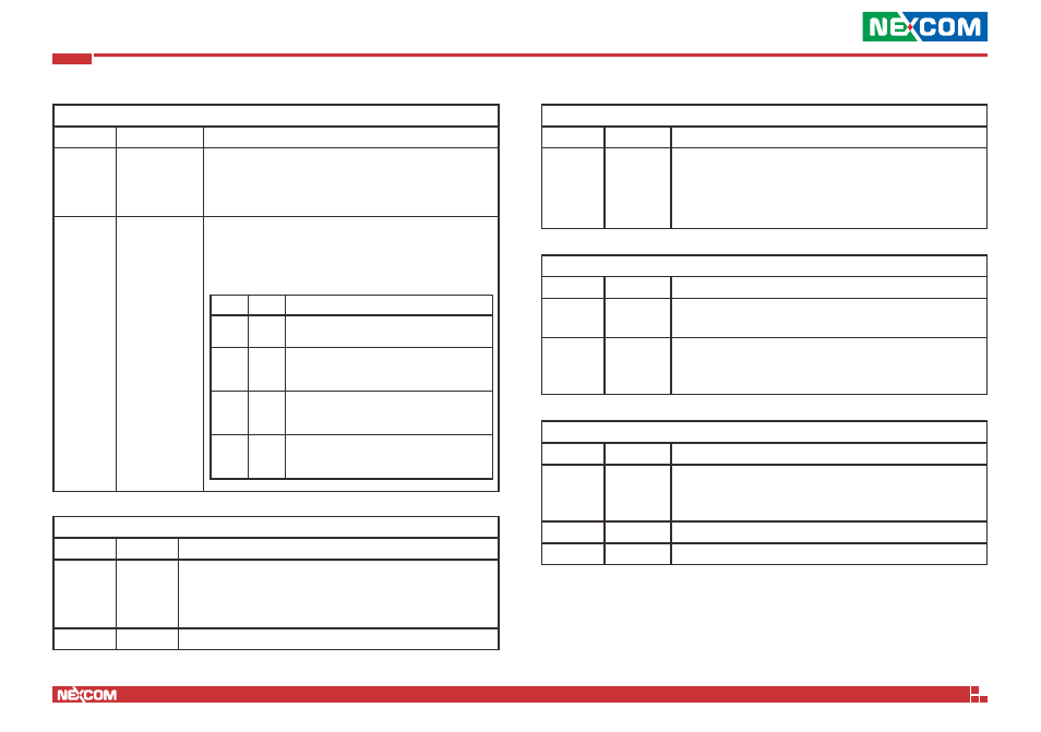
Appendix A: Bypass Register
Power ON State Bypass Control Status Register: F3
Bit Field
Name
Value
5:0
Segment 6 to 1
Segment bypass function control on Power ON state.
Bit[x] corresponds to segment[x+1], ex:
Bit0 control to segment1, … Bit5 control to segment6
0 = Segment[x] disable
1 = Segment[x] enable
7:6
Bypass Mode
These two bits defined the bypass in timer mode or force mode.
Note: The timer will recount while read/write F3 register
Limitation: Changing F3 segment bit during timer counting, the
timing mode segment will controlled by last change value.
Bypass Mode Table:
Bit 7
Bit 6
Action
0
0
Timer Disable:
Disable Timer mode function.
0
1
Force Enable:
Engage bypass relays on segments enable in
segment mask.
1
0
Force Disable:
Disable bypass relays immediately on segments
enabled in mask.
1
1
Timer Enable:
Segments enabled in mask are under Timer
control.
Power OFF State Bypass Control Status Register: F7
Bit Field
Name
Value
5:0
Segment 6
to 1
Segment bypass function control on Power OFF state.
Bit[x] corresponds to segment[x+1], ex:
Bit0 control to segment1, … Bit5 control to segment6
0 = Segment[x] disable
1 = Segment[x] enable
7:6
Unused
Unused.
Slot Select Register: F9
Bit Field
Name
Value
7:0
Slot ID bit 7
to 0
Main board: The bypass function workable while Slot ID set to
0x00h
Lan module: The bypass function workable while Slot ID value
meet H/W setting, The value do not set to 0x00h
Note: If all of boards not fill slot id value on platform, read all
registers will return 0xFF
PCB and CPLD Release Version Register (MSB): FD
Bit Field
Name
Value
3:0
CPLD version
MSB
CPLD version MSB, for CPLD release version control, the LSB info
at address ‘F1’, Read only
7:4
CPLD dot /
PCB
version MSB
The value >= “A” is CPLD dot version information. The value <
“A” indicate PCB version MSB, Read only
Bypass Timer/Force Mode Control Register: FE
Bit Field
Name
Value
0
Timer/force
mode
independent
0 = Timer/force mode dependent, the timer will stop in force
mode condition.
1 = Timer/force mode Independent, the timer will stop in timer
disable condition.
3:1
Unused
Unused
7:4
New CPLD
Always read “0xa”, Read only