BECKHOFF AX570x User Manual
Page 2
Seite 2/4
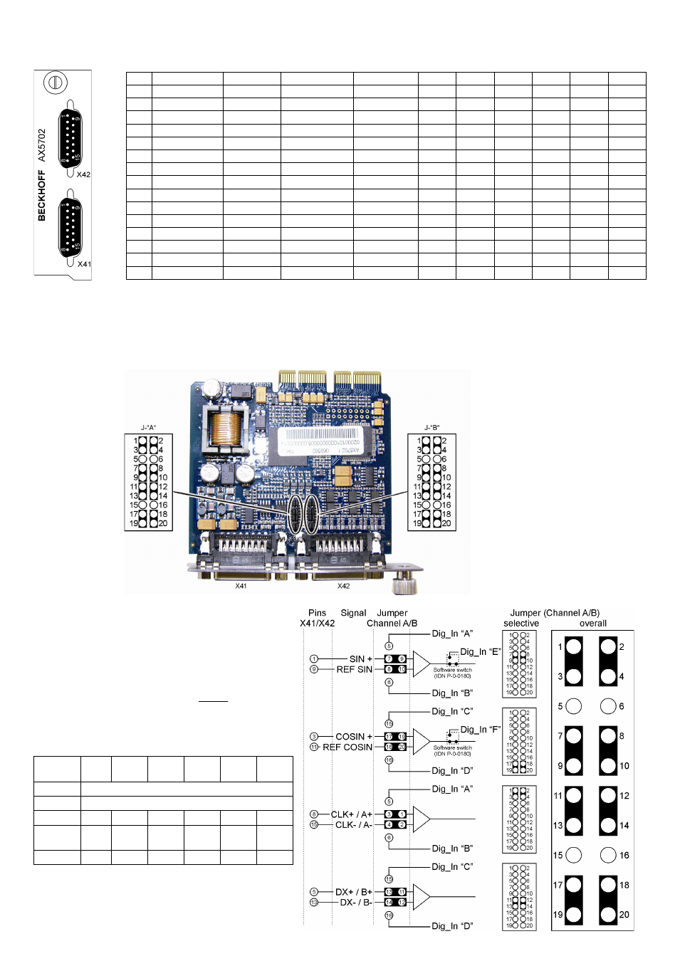
Overview of sockets X41 (channel A) and X42 (channel B)
Pin EnDAT / BiSS Hiperface Sin / Cos 1V
pp
TTL
In „A“ In „B“ In „C“ In „D“ In „E“ In „F“
1
SIN +
SIN +
SIN +
n.c.
X
X (+)
2
GND_5 V
GND_9 V
GND_5 V
GND_5 V
3
COS
COS
COS
n.c.
X
X (+)
4
U
S
_5 V
n.c.
U
S
_5 V
U
S
_5 V
5
DX+ (Data)
DX+ (Data) n.c.
B+
Y
6
n.c.
U
S
_9 V
n.c.
n.c.
7
n.c.
n.c.
REF Z
REF Z
8
CLK+ (Clock)
n.c.
n.c.
A+
Y
9
REFSIN
REFSIN
REFSIN
n.c.
X
X (-)
10
GND_Sense
n.c.
GND_Sense
GND_Sense
11
REF COS
REF COS
REF COS
n.c.
X
X (-)
12
U
S
_5 V Sense n.c.
U
S
_5 V Sense
U
S
_5 V Sense
13
DX- (Data)
DX- (Data) n.c.
B-
Y
14
n.c.
n.c.
Z
Z
15
CLK- (Clock)
n.c.
n.c.
A-
Y
The digital inputs “A” to “D” can be connected to X or Y.
The digital inputs “E” and “F” must be connected to X (+) and X (-).
Configuration of jumpers J-“A” for channel “A” and J-“B” for channel “B”
Jumpers J-“A” and J-“B” (1) are located at the centre of the printed circuit board near the front panel of the card. For each channel there are 2 row of
jumpers, each with 20 pins. The default setting without analysis of the additional inputs is shown in the following figure.
The opposite figure shows the basic jumper configuration, which
is the same for channel A and channel B. The pins of input
sockets X41 and X42 are wired firmly to the corresponding pins
of the jumpers rows. The non-configurable pins are not shown.
To use the additional inputs proceed as follows:
•
Reposition the relevant jumpers und set IDN P-0-
0180Feedback optionsDigital Inputs “
Input A” to “Input D”
to “
used” or set IDN P-0-0180Feedback optionsDigital
Inputs “
Input E” or “Input F” to “used” without repositioning
the jumpers.
•
Connect the encoder cable as required for the relevant inputs
or use an adapter.
The following table shows a selection of combination options.
Feedback
system
Input
“A”
Input
“B”
Input
“C”
Input
“D”
Input
“E”
Input
“F”
EnDAT
Input “A-F” not available
BiSS
Input “A-F” not available
Hiperface
X
X
Sin / Cos
1V
pp
X
X
X
X
TTL
X
1
X
1
X
2
X
2
X
1
X
2
1)
Either inputs “A” and “B” or
input “E” can be used.
2)
Either inputs “C” and “D” or
input “F” can be used.