Comtech EF Data PCB-4300 User Manual
Page 24
PCB-4300 1:2 Phase Combiner
Revision 2
External Connectors
MN/PCB4300.IOMMN/PCB4300.IOM
2–2
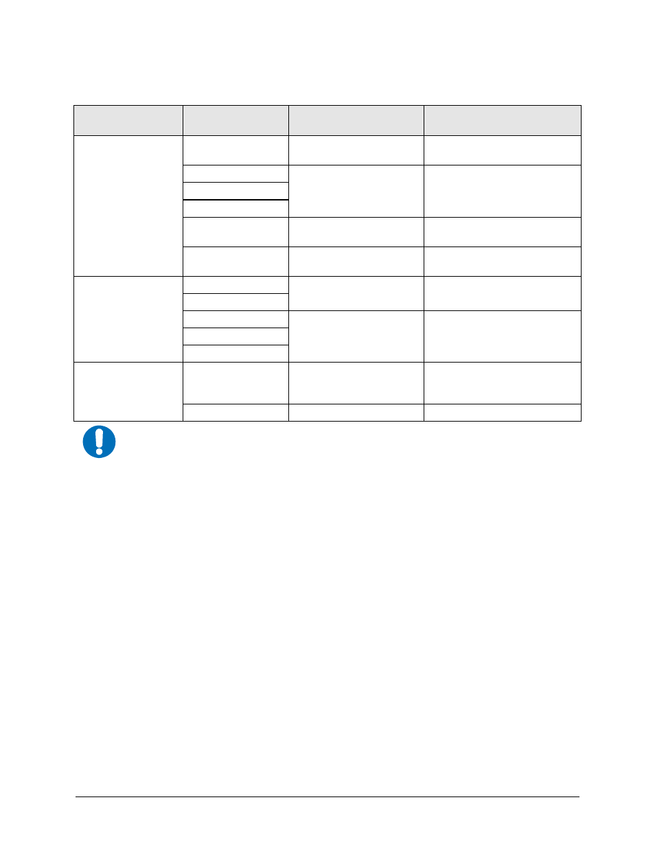
Table 2-1. PCB-4300 External Connectors
Connector Group
(Chapter Sect.)
Name / Ref Des
Connector Type
Function
M&C (Sect. 2.2)
SYSTEM COM J1
19-pin Circular Connector
Customer EIA-232/485 and discrete
interface
SSPA COM 1 J2
19-pin Circular Connector
Connects to SSPAs
SSPA COM 2 J3
SSPA COM 3 J4
SSPA SW OUT J5
19-pin Circular Connector
Connects to both waveguide
switches
RF INPUT SWITCH J6
6-pin Circular Connector
Drive input, selects either RF IN 1 or
RF IN 2
RF (Sect. 2.3)
RF IN 1 J7
Type ’N’
RF Inputs to PCCB
RF IN 2 J8
SSPA OUT 1 J9
Type ’N’
RF Outputs to SSPAs
SSPA OUT 2 J10
SSPA OUT 3 J11
Power/Ground
(Sect 2.4)
AC
Pin ‘R’ on SSPA COM 1 J1,
SSPA COM 2 J3, SSPA COM
3 J4
See Sect. 2.4.1 for AC power
provision note
Ground
#10-32 stud
Common Chassis Ground
IMPORTANT
To maintain compliance with the European EMC Directive (EN55022, EN50082-1)
properly shielded cables are required for data I/O.