8 virtex4 fpga bank allocation, Virtex4 fpga bank allocation – Sundance SMT148FX User Manual
Page 29
Advertising
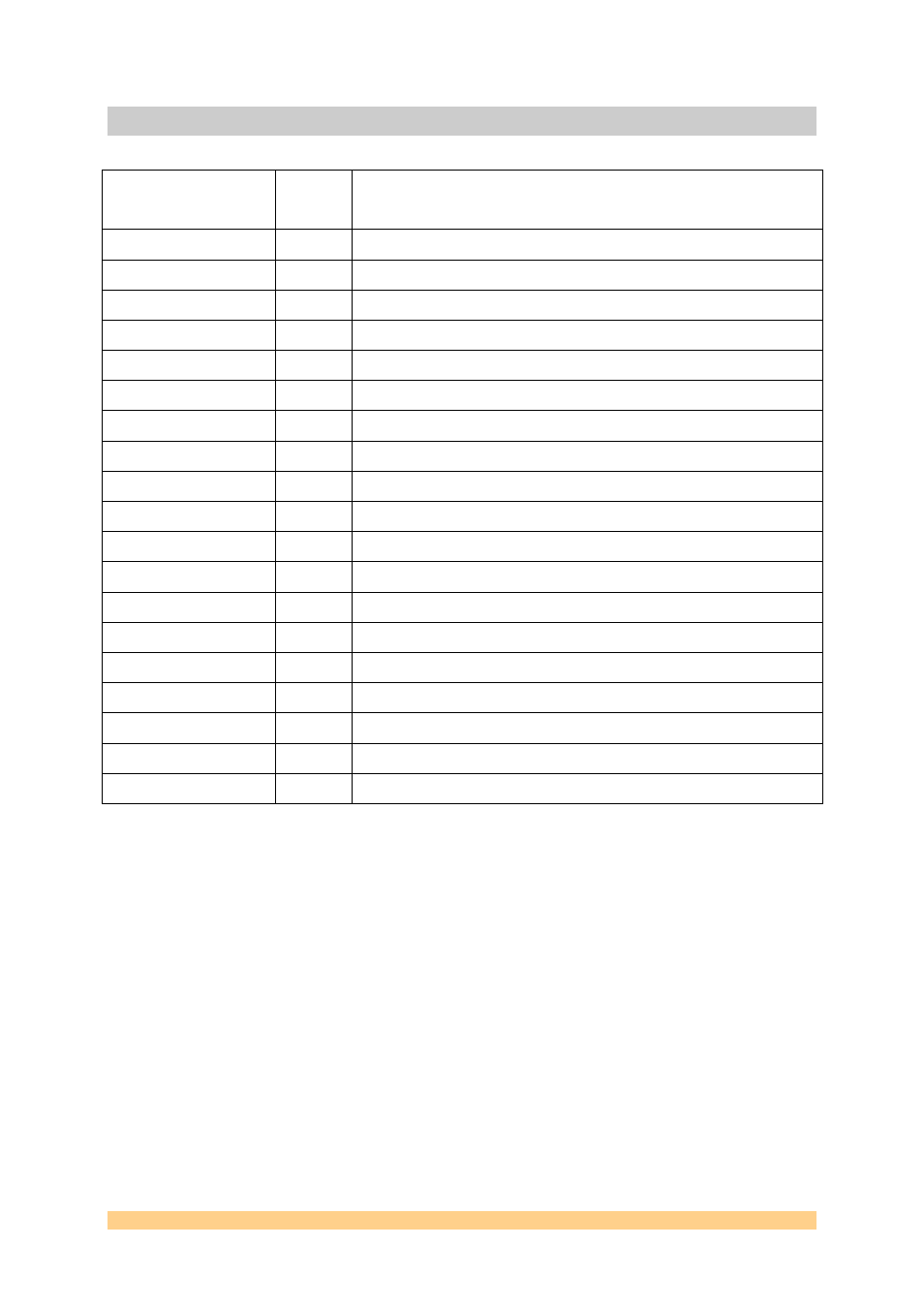
8 Virtex4 FPGA Bank Allocation
Interface Bank
Comment
Global Bus A
5
12 Address, 16 Data, 4 Control (STRB, RDY, WR, PAGE)
Global Bus B
6+10
12 Address, 16 Data, 4 Control (STRB, RDY, WR, PAGE)
Global Bus C
8
12 Address, 16 Data, 4 Control (STRB, RDY, WR, PAGE)
Global Bus D
11
12 Address, 16 Data, 4 Control (STRB, RDY, WR, PAGE)
ZBT Bank 1
10
Clock uses GCK on bank
ZBT Bank 2
12
Clock uses GCK on bank
Ethernet 12
SHB 7
RS485
7+8
Direction control is on bank 8.
ComPorts
11+5
2 ports per bank used.
LVDS 9
USB
8
Appears as a 16 bit SDB.
LEDs 5+9
Misc, TIM
1+3+4
RS232 5
Tx,
Rx.
RST, Clock
5
IEEE1394 6
TIM reset
11
V4 to S3 interface
8
CLK, DATA, LOAD, RESET
User Manual SMT148FX
Page 29 of 48
Last Edited: 03/08/2009 11:42:00
Advertising