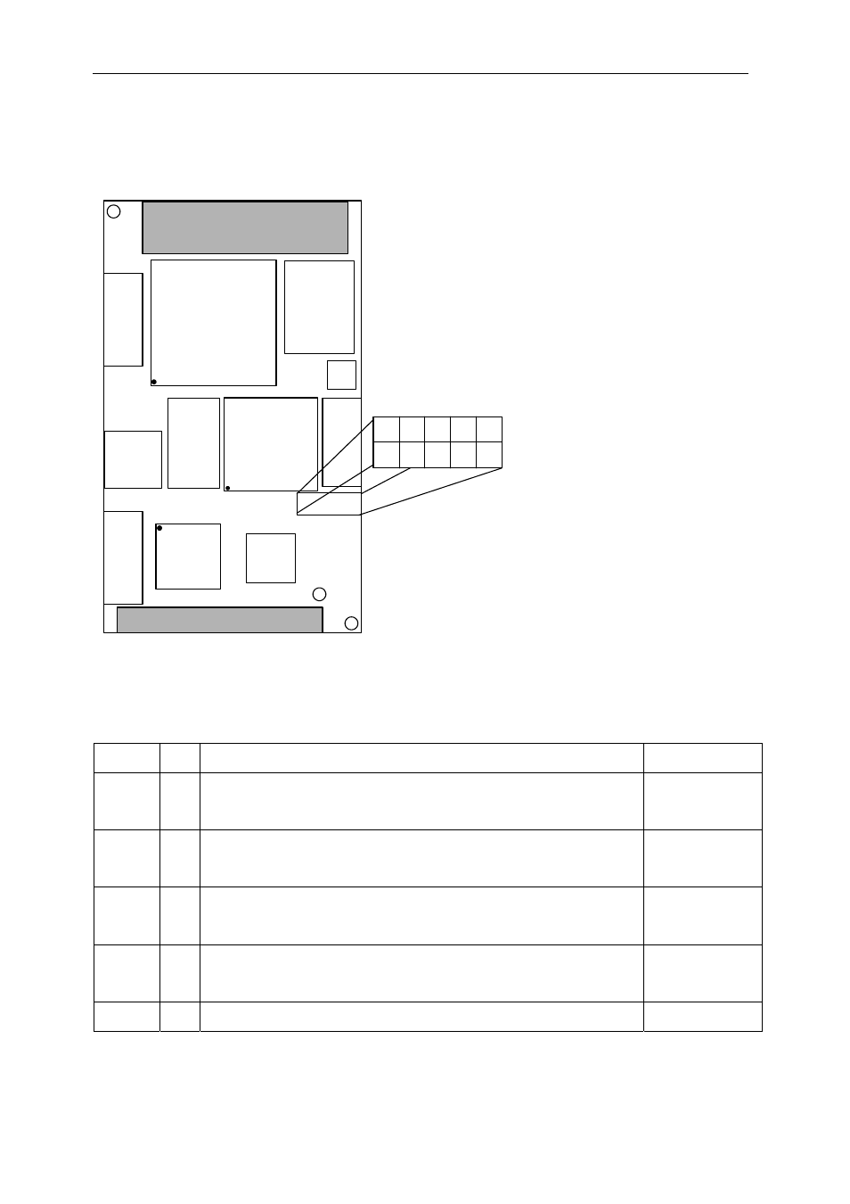
Jtag/multilinx headers, Figure 13: top view of jtag/multilinx headers, See board header pinout in – Sundance SMT387 User Manual
Page 40: Table 9: connector jtag/jumper header
Advertising
Version 1.0.3
Page 40 of 42
SMT387 User Manual
JTAG/Multilinx headers
The JTAG/Multilinx headers have the following pinout:
TIM Connector
TIM Connector
2.5
V
SDR
A
M
IP1001
1.5V
S-ATA
XCVR
XC9536
VQ44
320C6415
DSP
XC2VP
FF896
S
H
B
R
S
L
S
A
T
A
ZBT
SRAM
HDR
9
7
5
3
1
10
8
6
4
2
Figure 13: Top View of JTAG/Multilinx headers
JTAG Boundary scan/User defined jumpers pinout (JP1/JP2)
Name Pin Function
Connections
JMP1 1
User defined function
Pulled-up to 3.3V with 4.7k when unconnected
To FPGA pin
AD16
JMP0 2
User defined function
Pulled-up to 3.3V with 4.7k when unconnected
To FPGA pin
AE16
GND 3 Ground
Designed to pull down pin 1 by using a 0.1” jumper.
Board
ground
GND 4 Ground
Designed to pull down pin 2 by using a 0.1” jumper.
Board
ground
VCC 5 Power.
To
target
VCC
Advertising