Smt700 block diagram, Smt784 functional description, Figure 1: smt700 block diagram – Sundance SMT784 v.1.0 User Manual
Page 9
Version 1.0
Page 9 of 31
SMT784 User Manual
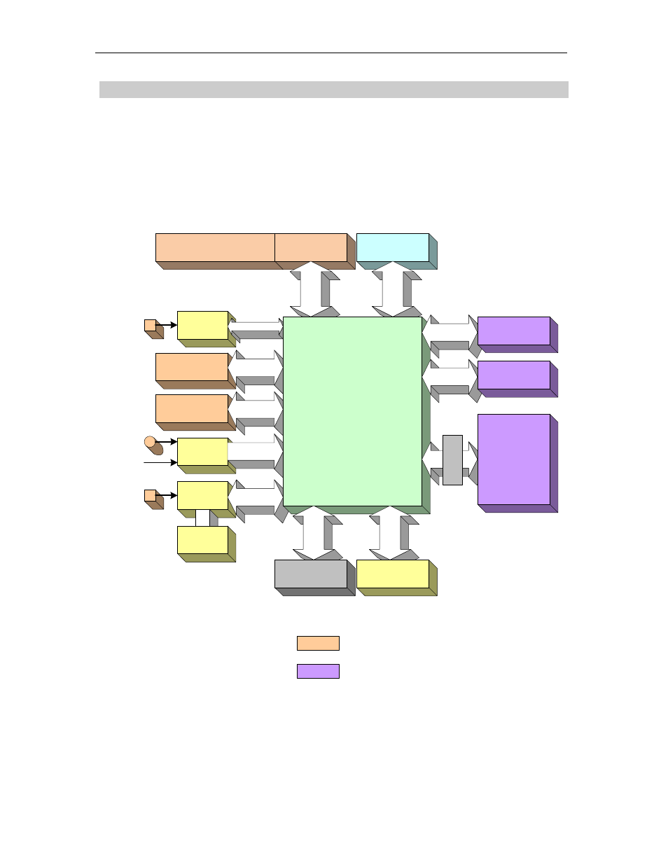
SMT784 Functional Description
The major elements of the SMT784 can be broken down into the two main modules it
is comprised of: the SMT700 and SMT384. The SMT700 PXIe carrier board block
diagram can be viewed below.
Custom Front Panel
Ethernet
PHY
SFF Connectors
2 lanes of Fibre
2 x 2.5Gb/s
serial links
Config
CPLD
& USB
Clock
generation
1.5GHz SATA
2.5GHz RSL
SATA Connectors
2 lanes of RSL
DDR2
1GByte 220MHz
SLB
1
20 I/
O
pi
ns
FPGA
Virtex5 LXT-50
FF1136 package
PXIe Connector
8 lanes of 2.5Gb/s
8 x 2.5Gb/s
serial links
64
b
it
d
a
ta
19
ad
d
res
s
13 con
tr
o
l
PXI Control
(Trigger, Clk, etc)
32 bit PCI
33/66MHz
(option)
2 x 2.5Gb/s
serial links
Ext clk
USB
PXIe ref
512Mbit
flash
RSL Connector
4 lanes of 2.5Gb/s
4 x 2
.5G
b
/s
ser
ia
l l
in
ks
LEDs and
Misc. I/O
SHB
(opti
o
n
)
Front Panel
Connector
Rear Card
Connector
SMT700 Block Diagram
Ethernet
Figure 1: SMT700 Block Diagram