Block diagram, Xilinx fpga – Sundance SMT363XC2 User Manual
Page 8
Version 2.2
Page 8 of 27
SMT363XC2 User Manual
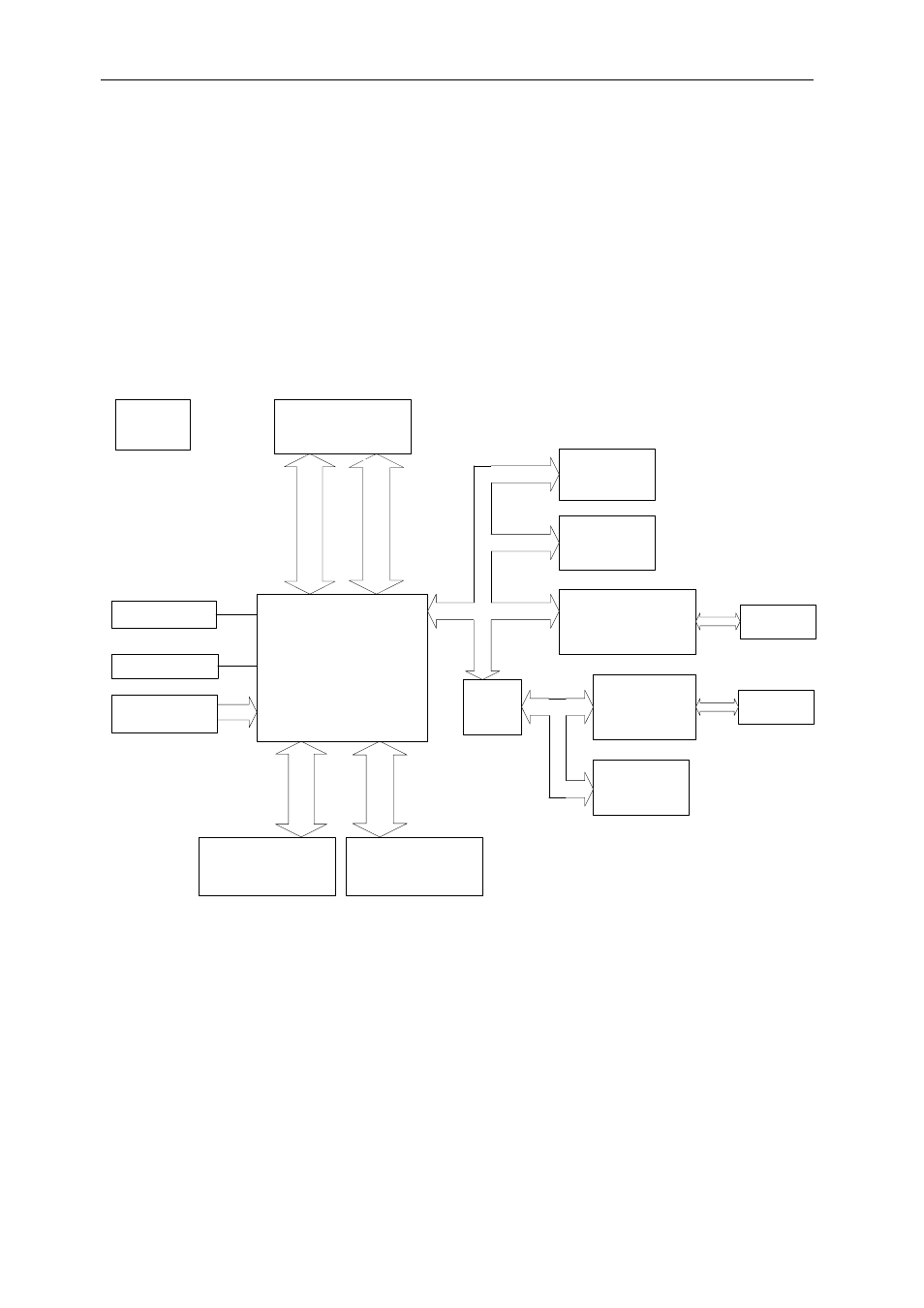
Block Diagram
The following drawing shows the block diagram of the SMT363XC2 module.
The main components of the SMT363XC2 are:
- A Texas Instruments DSP
- One Xilinx Virtex-II FPGA
- One NetSilicon ARM Net+50 device with integrated MAC controller for
connection to an Ethernet network.
- 16/64MB of SDRAM
2
x C
o
m
m
-P
ort
s/SD
L
2
4 I
/O
pi
ns
T
im
e
r,&
C
o
n
tro
l
1
5 I
/O
pi
ns
4x
C
o
m
m
-P
ort
/SD
L
4
8
I
/O
pi
ns
Gl
ob
al
Bus
7
4
I
/O
pi
ns
Xilinx FPGA
Virtex-II
1.5V
JTAG Header
J1 Top Primary TIM
Connector
Comm-Port 3
J3 Global Expansion
Connector
J2 Bottom Primary TIM
Connector
Comm-Port 1, 2, 4
DSP and
FPGA PSU
Sundance High-speed
Bus
60-way Samtec
4 LEDs &
4 I/O pins
16M bytes SDRAM
2 x (4M x 16)
'C6211/6711/6713
DSP
McBSP,
GPIO, LEDs
16/64M bytes
SDRAM
2 x (4/16M x 16)
8M bytes Flash
32-bit EMIF
NET+50
Dual Port
RAM
RJ45, RS232,
LEDs
Figure 1: SMT363XC2 block diagram