Block diagram, Fpga controller – Sundance SMT365E User Manual
Page 7
Version 2.1
Page 7 of 26
SMT365e User Manual
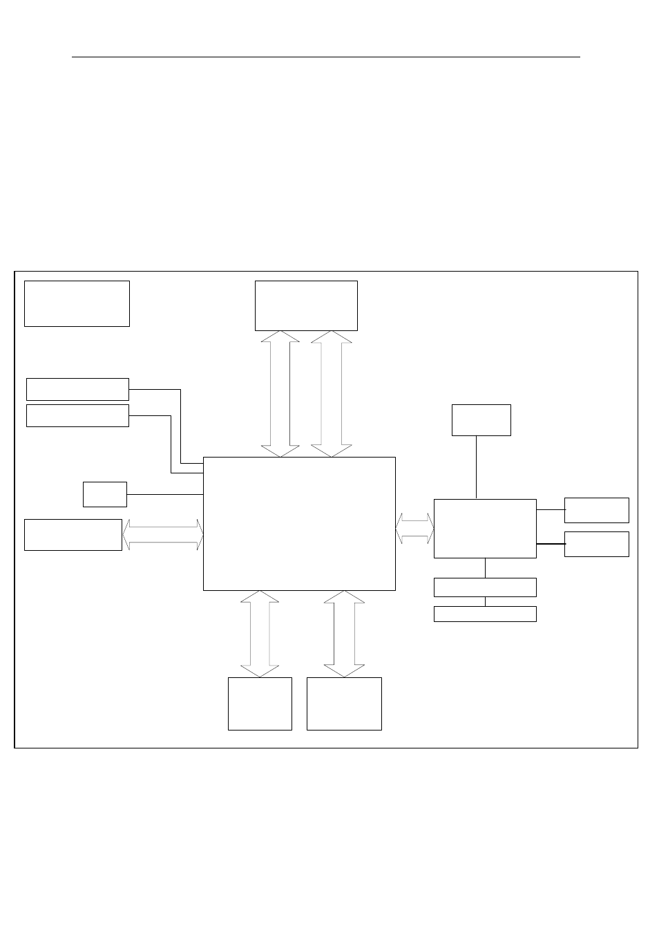
Block Diagram
The following drawing shows the block diagram of the SMT365e module.
The main components of the SMT365e are:
- A Texas Instruments DSP
- One Xilinx FPGA Virtex-II device
- 256MB of SDRAM
Sundance High-speed Bus
60-way Samtec x 6
2x C
o
mm-Ports/SDL
26 I/O p
ins
Tim
e
r,&
Cont
rol
15 I/O p
ins
4x
C
o
mm
-Por
t/S
D
L
52
I/O
pins
Gl
o
b
a
l B
u
s
74
I/O
pins
360 pins
FPGA Controller
Virtex-II, FF1152
824 I/O pins - Used 776
XC2V6000
1.5V
'C6416
DSP
525 pins
256Mbytes SDRAM
JTAG Header
X-Checker Header
J1 Top Primary TIM
Connector
Comm-Port 0 & 3
J3 Global
Expansion
Connector
J2 Bottom Primary
TIM Connector
Comm-Port 1;2;5;4
McBSP/Utopia/
GPIO
4 LEDs &
4 I/O pins
Flash
4 LEDs
+ GPIO
Oscillator
DC-DC Converters for DSP
and FPGA cores
171 pins