Switch sw1 – Verilink 4010 DDS CSU/DSU (Chassis) (CG) Configuration/Installation Guide User Manual
Page 2
1 - 3 Channel Bit Rate Select: These three positions select the channel bit rate (refer to
the table on the right). The RTS-to-CTS delays are multiplied by two when SW1-10 is
in the B position.
4
Line Clock: This position selects either an internal clocking source or a loop timing
source from the received data.
5
Internal Clock: This position selects either the DSU external clock input or the crystal
oscillator as the clocking source. It is applicable only if SW1-4 is in the B position.
6
V.54 Loop Operation: This position enables or inhibits V.54 loop operation.
7
Data Polarity: This position determines whether data bits are inverted. In the A position,
marks equals pulses. In the B position, spaces equal pulses. Receipt of OOF, OOS, idle, or
loop codes forces the DSU data to all marks (A position) or spaces (B position).
8
Circuit Assurance: On allows the status of CF (receive line signal detector) and CA
(request to send) to control the output CB (clear to send). If either CA or CF is Off (A
position), CB is Off. If CA and CF are On (B position), CB is On.
9
RTS /CTS Control: In the B position, CTS is forced On regardless of the RTS input
status. In the A position, delays are determined by SW1-10.
10
RTS-to-CTS Delay: In the A position, the RTS-to-CTS delay is as shown in the bit
rate table of the diagram. In the B position, the delays shown are multiplied by two.
Ckt. V.35 RS-232
Signal Name - Function
DCE
101
A
1
Frame Ground - This circuit is used to terminate shields.
Gnd
102
B
7
Signal Ground - This circuit is used as the return reference for unbalanced signals.
Gnd
103
P/ S
2 / 14 Transmit Data - This input is used for synchronous TD from the DTE. It is transmitted on the DDS side.
In
104
R /T
3 / 16 Receive Data - This output is the data decoded from the incoming DDS receive data.
Out
105
C
4
Request To Send - This input is a control line from the DTE, indicating data is to be transmitted. When RTS
is ON (space), the data transmitter, the zero suppression circuitry, and the CTS are enabled. When RTS is
OFF, the transmitter sends idle code and the CTS is forced OFF.
In
106
D
5
Clear To Send - This output is a DCE response, indicating that either RTS is ON or SW1 - 9, position B, is
forcing RTS ON. When SW1 - 8 is in position B, RTS and RLSD must be ON for CTS to be ON.
Out
107
E
6
Data Set Ready - This output is ON when the unit is not in a test mode (other than a V.54 test).
Out
109
F
8
Data Carrier Detect - This output is ON when the correct data or zero suppression code is being received
and DSR is ON. It is OFF when either DSR is OFF, the DDS receiver has lost sufficient signal to operate
for at least one second, or the receiver has received OOS, OOF, idle, or loop codes for about 20 U.I.
Out
113
U /W 24 / 11 External Transmit Clock - This is the synchronous transmit clock input from the DTE. When both SW1-4 and
SW1-5 are in the B position, this clock controls the frequency of the DDS transmit clock and clocks circuit 103
(TD). When either SW1-4 or SW1-5 is in the A position, this input has no effect on DDS operation.
In
114
Y/AA 15 / 12 Transmit Clock - This output is supplied by the DCE as an external DTE timing source. It is generated from the
internal data clock or the far-end transmit data. Not available if SW1-4 and S1-5 are in the B position.
Out
115
V /X
17 / 9 Receive Clock - This clock output is the timing for the RD and is always used to time the receive data. This
clock is always derived from the DDS receive data.
Out
Note: When two pins are listed, RS-232 uses the first pin. All pins not specified are open.
Notes:
Standard Equipment: A cable is supplied for the NET
connector which puts the DDS signal on the proper pairs.
The TxPORT part number is 9-1001-069-1. If this cable
is not used, the DDS output (TX) is on pins 4 and 5 and
the DDS input (RX) is on pins 1 and 2 of the T1 network
connector.
DTE Interface: The rear of the circuit card has Switch
S1 and Switch S2 which are used to select the type of
DTE interface. Move both switches to the V.35 position to
select a V.35 interface (factory default) or move both
switches to the 232 position to select an RS-232 interface.
Factory Defaults: The A position is the factory default
for Switch SW1 settings. If a particular user configura-
tion requires that a switch be placed in the B position,
then mark this sheet for future reference.
6
5
4
3
1
7
9
8
2
Da
ta
P
o
la
rit
y
Circuit
As
su
rance
R
T
S
/CT
S
Cont
rol
Da
ta
Pola
rity
Cir
cuit As
su
rance
R
T
S
Nor
m
al
Delay
Channel
Bit Rate
A
B
V
.54 L
oop
V
.54 L
o
o
p
In
ternal Clock
L
ine
Clock
In
v
ert
ed
Nor
m
al
Of
f
On
En
ab
le
d
Inhi
bited
R
T
S
/CT
S Contro
l
R
T
S Contr
o
l On
R
T
S-
to-C
T
S
De
la
y
×
2
R
T
S
-to
-C
TS
D
ela
y
Nor
m
al
The symbol
indicates that the switch pointed to does not func-
tion unless the opposite end of the arrow is in the position shown. For
example, SW1 -5 does not function unless SW1 - 4 is in the B position.
B
A
A
n/a
Master
Network (slave)
B
B
External
TxPORT
127 Jetplex Circle
Madison, Alabama 35758
Customer Service
800-926- 0085, ext. 2227
888-4TxPORT, ext. 2227
Product Technical Support
(8 a.m. to 5 p.m. Central)
888-4TxPORT,
800- 285-2755, or
205-772- 3770
Emergency After Hours
800-285- 2755
E-Mail (Internet Address):
V.35 and RS-232 Interface
Switch SW1 Description
T1 DTE
1
2
3
4
5
6
7
8
9
10
11
12
( B )
NMS
IN
( B )
NMS
OUT
12
High Speed DTE
11
10
9
8
7
6
5
4
3
2
1
T1 NET
TB1
TB2
ENET
( A )
NMS
IN
( A )
NMS
OUT
TB1
TB2
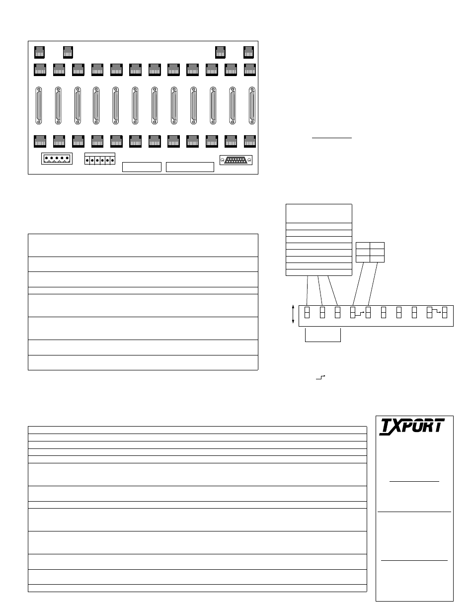
TxPORT 1051-2 Chassis Rear View
1
2
3
4
5
6
7
8
9
10
11
12
10
Rate
(kbps)
1
2
3
RTS-
to-CTS
Delay
2.4
B
B
B 8 ms
4.8
A
B
B 4 ms
9.6
B
A
B 2 ms
19.2
A
A
B 1 ms
28
B
B
A 0.8 ms
38.4
A
B
A 0.5 ms
56
B
A
A 0.4 ms
64
A
A
A 0.3 ms
The RS-232 version of the chassis is shown. The V.35 version is also available.
The 4010 DDS CSU/DSU is only for use in the TxPORT-model 1051 chassis.
Switch SW1
T
R
A
N
S
P
O
R
T
®