Chapter 3, Board layout – Lanner LVC-2000 User Manual
Page 18
18
Board Layout
Chapter 3
Embedded and Industrial Computing
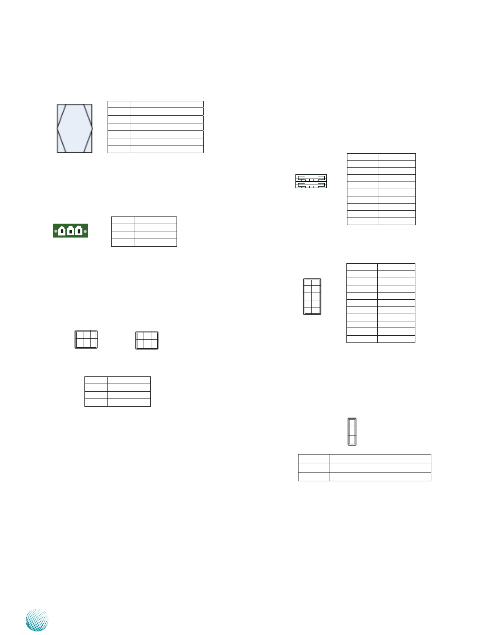
SIM Card Socket (SIM1): SIM1 pairs with MPCIE1 and
SIM2 pairs with MPCIE2.
Power-in with Ignition Control (PRJK1): A power
connector with power -ignition Control
COM1/COM2 Power Selection (JRI1/JRI2): JRI1 selects
COM1 power voltage and JRI2 selects COM2 power voltage
. The default is Ring Indicator (RI) for pin 8.
USB 2.0 Pin Header for USB 0, USB1 (USBF1)
USB 3.0 Port Connector for USB2 (USB2)
Clear CMOS (JCMOS1):
Pin No.
Pin Name
1
Ignition
2
GND
3
DC_VIN
3 2 1
1 2 3 4
5 6 7 8
Pin No.
Pin Name
1
VCCUSB2
2
USB0N2
3
USB0P2
4
GND
5
USB3_SSRXN
6
USB3_SSRXP
7
GND
8
USB_SSTXP
9
USB_SSTXN
Pin No.
Pin Name
1-2
Normal (Default)
2-3
Clear RTC
Pin No.
Description
C1
UIM_PWR
C2
UIM_RST
C3
UIM_CLK
C5
GND
C6
UIM_VPP
C7
UIM_DAT
C5 C7
C1 C3
Pin No.
Pin Name
1
VCC5
2
GND
3
N/A
4
USBDDP1
5
USBDN0
6
USBDN1
7
USBDP0
8
N/A
9
GND
10
VCC5
1
3
5
7
9
2
4
6
8
10
2
1
6
5
JRI1
2
1
6
5
JRI2
Pin No.
Signal
1-2
Default
3-4
VCC5
5-6
VCC12