Chapter 3: motherboard information, Block diagram, Chapter 3 – Lanner FW-6432 User Manual
Page 9: Motherboard information
Advertising
6
Motherboard Information
Chapter 3
Network Application Platforms
Chapter 3:
Motherboard Information
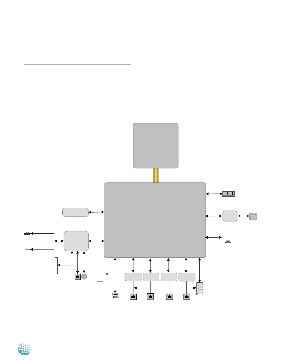
Block Diagram
The block diagram depicts the relationships among the
interfaces or modules on the motherboard. Please refer
to the following figure for your motherboard’s layout
design.
VIA Eden ULV
500MHz
VIA
VX900
LPC
4x GbE RJ-45
4x PCI-E x1
Compact Flash
2x pin
headers
USB 2.0
Onboard DDR3
512MB
Realtek
8111E
Winbond
83627DHG
GPIO
Fan Monitor
Thermal Monitor
SPI
Front
LED
Realtek
8111E
Realtek
8111E
Realtek
8111E
Watchdog
SA
TA
II
VGA
D
D
R3
RJ45
Console
LCM/Key Pad
KB/Mouse
2x USB
Connectors
VGA pin
headers
SPIF223
Reset
Button
FSB 400MHz
Advertising