Microstrip details, Production guidelines, Hand assembly – Linx Technologies RXM-GPS-R4 User Manual
Page 17: Automated assembly, Castellations pcb pads soldering iron tip solder
–
–
–
–
28
29
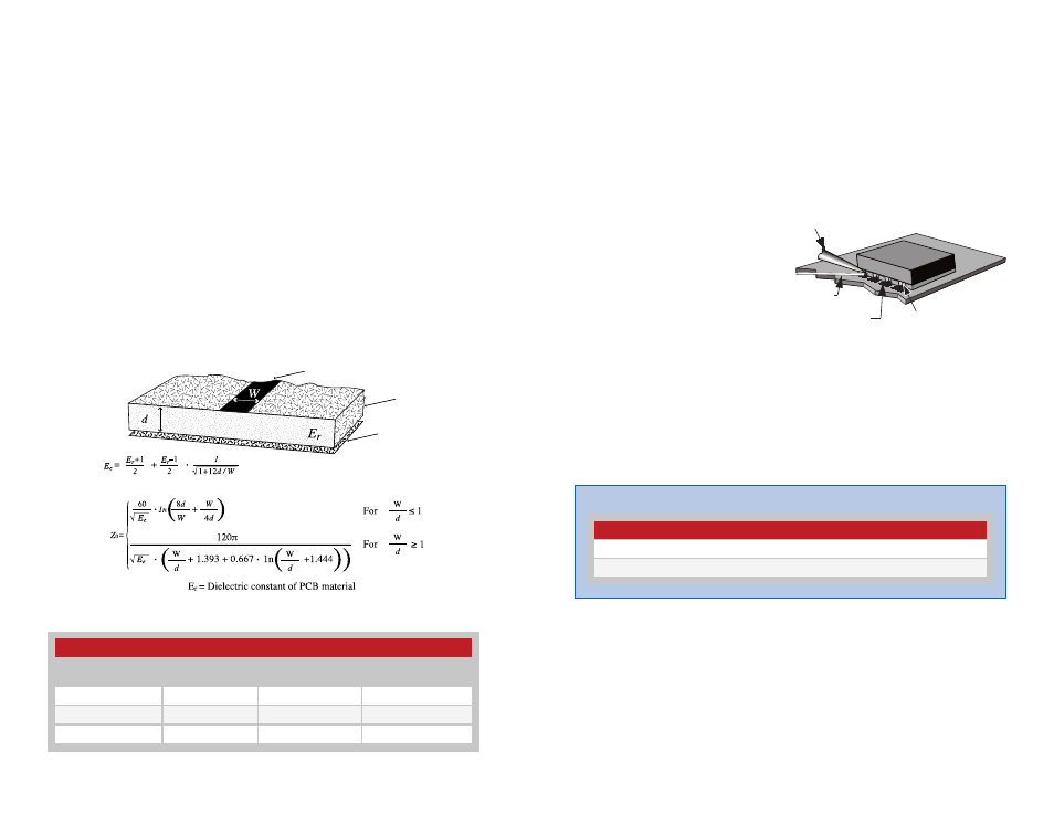
Microstrip Details
A transmission line is a medium whereby RF energy is transferred from
one place to another with minimal loss. This is a critical factor, especially in
high-frequency products like Linx RF modules, because the trace leading
to the module’s antenna can effectively contribute to the length of the
antenna, changing its resonant bandwidth. In order to minimize loss and
detuning, some form of transmission line between the antenna and the
module should be used unless the antenna can be placed very close (<
1
⁄
8
in)
to the module. One common form of transmission line is a coax cable and
another is the microstrip. This term refers to a PCB trace running over a
ground plane that is designed to serve as a transmission line between the
module and the antenna. The width is based on the desired characteristic
impedance of the line, the thickness of the PCB and the dielectric constant
of the board material. For standard 0.062in thick FR-4 board material, the
trace width would be 111 mils. The correct trace width can be calculated
for other widths and materials using the information in Figure 32 and
examples are provided in Figure 33. Software for calculating microstrip lines
is also available on the Linx website.
Trace
Board
Ground plane
Example Microstrip Calculations
Dielectric Constant
Width/Height
Ratio (W/d)
Effective Dielectric
Constant
Characteristic
Impedance (Ω)
4.80
1.8
3.59
50.0
4.00
2.0
3.07
51.0
2.55
3.0
2.12
48.0
Figure 32: Microstrip Formulas
Figure 33: Example Microstrip Calculations
Production Guidelines
The module is housed in a hybrid SMD package that supports hand and
automated assembly techniques. Since the modules contain discrete
components internally, the assembly procedures are critical to ensuring
the reliable function of the modules. The following procedures should be
reviewed with and practiced by all assembly personnel.
Hand Assembly
Pads located on the bottom
of the module are the primary
mounting surface (Figure 34).
Since these pads are inaccessible
during mounting, castellations
that run up the side of the
module have been provided to
facilitate solder wicking to the
module’s underside. This allows
for very quick hand soldering
for prototyping and small volume production. If the recommended pad
guidelines have been followed, the pads will protrude slightly past the
edge of the module. Use a fine soldering tip to heat the board pad and the
castellation, then introduce solder to the pad at the module’s edge. The
solder will wick underneath the module, providing reliable attachment. Tack
one module corner first and then work around the device, taking care not
to exceed the times in Figure 35.
Automated Assembly
For high-volume assembly, the modules are generally auto-placed.
The modules have been designed to maintain compatibility with reflow
processing techniques; however, due to their hybrid nature, certain aspects
of the assembly process are far more critical than for other component
types. Following are brief discussions of the three primary areas where
caution must be observed.
Castellations
PCB Pads
Soldering Iron
Tip
Solder
Figure 34: Soldering Technique
Figure 35: Absolute Maximum Solder Times
Warning:
Pay attention to the absolute maximum solder times.
Absolute Maximum Solder Times
Hand Solder Temperature: +427ºC for 10 seconds for lead-free alloys