Power supply requirements, Protocol guidelines – Linx Technologies RXM-xxx-ES User Manual
Page 9
– –
– –
12
13
higher than the reference voltage before switching on. This prevents low
amplitude noise from causing the data line to oscillate. Strong signals can
still get through, so it is a good idea to have a noise tolerant protocol.
Creating a circuit that has additional hysteresis characteristics is very
basic and requires very few parts thanks to the A REF line. All you need
are a couple resistors to provide some isolation for the AUDIO and A REF
lines, a large feedback resistor, a pull-up resistor, and an open collector
comparator.
The RSSI and A REF lines allow a wide variety of squelch circuits to be
implemented. One such possibility is the circuit in Figure 13, which is used
on the ES Series Master Development System, and may be employed for
audio or data squelching. It is ultimately the responsibility of the designer to
determine what, if any, circuit would be most appropriate for the needs of
the product.
Data squelching in the circuit above is accomplished by comparing the
RSSI voltage to a voltage reference (typically a voltage divider) with an open
collector style comparator. When the voltage from the RSSI becomes lower
than the voltage reference, the comparator output is pulled to GND. This
is useful because this output can be used to disable the data-slicer circuit
either when the receiver is out of range or the transmitter is turned off.
The squelch threshold is normally set as low as possible to ensure
maximum sensitivity and range. It is important to recognize that in many
actual use environments, ambient noise and interference may enter the
receiver at levels well above the squelch threshold. For this reason, it is
always recommended that the product’s protocol be structured to allow
for the possibility of hashing even when an external squelch circuit is
employed.
5k
Qualified Data
390k
RSSI
GND
GND
GND
GND
VCC
0.01uF
39k
10k
2M
39k
VCC VCC
AUDIO
AUDIO REF
2M
10k
10k
10k
LM393
8
VCC
7
OUTB
6
INB-
5
INB+
4
GND
3
INA+
2
INA-
1
OUTA
Figure 13: ES Series Receiver Squelch / Hysteresis Circuit
Power Supply Requirements
The module does not have an internal voltage
regulator; therefore it requires a clean,
well-regulated power source. While it is preferable
to power the unit from a battery, it can also be
operated from a power supply as long as noise
is less than 20mV. Power supply noise can affect
the transmitter modulation; therefore, providing
a clean power supply for the module should be a
high priority during design.
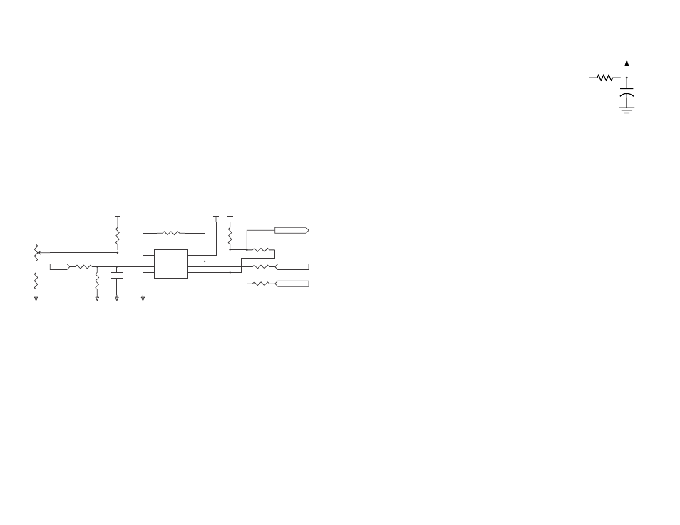
A 10
Ω resistor in series with the supply followed by a 10µF tantalum
capacitor from V
CC
to ground will help in cases where the quality of the
supply is poor. Note that the values may need to be adjusted depending on
the noise present on the supply line.
Protocol Guidelines
While many RF solutions impose data formatting and balancing
requirements, Linx RF modules do not encode or packetize the signal
content in any manner. The received signal will be affected by such factors
as noise, edge jitter, and interference, but it is not purposefully manipulated
or altered by the modules. This gives the designer tremendous flexibility for
protocol design and interface.
Despite this transparency and ease of use, it must be recognized that there
are distinct differences between a wired and a wireless environment. Issues
such as interference and contention must be understood and allowed for
in the design process. To learn more about protocol considerations, we
suggest you read Linx Application Note AN-00160.
Errors from interference or changing signal conditions can cause corruption
of the data packet, so it is generally wise to structure the data being sent
into small packets. This allows errors to be managed without affecting large
amounts of data. A simple checksum or CRC could be used for basic error
detection. Once an error is detected, the protocol designer may wish to
simply discard the corrupt data or implement a more sophisticated scheme
to correct it.
+
10
Ω
10
µF
Vcc IN
Vcc TO
MODULE
Figure 14: Supply Filter