Linx Technologies MDEV-LICAL-MS User Manual
Page 8
–
–
–
–
10
11
The PDN switch connects the RX_CNTL line of the encoder to the PDN line
of the receiver so that the RX Control Mode of the decoder can be tested.
This mode is described in the MS Series Decoder Data Guide.
The LATCH switch places the decoder into Latch Mode when on, so that
the data lines will go high when a valid signal is received and stay high
until a second valid signal is received. If the switch is off, the data lines are
momentary.
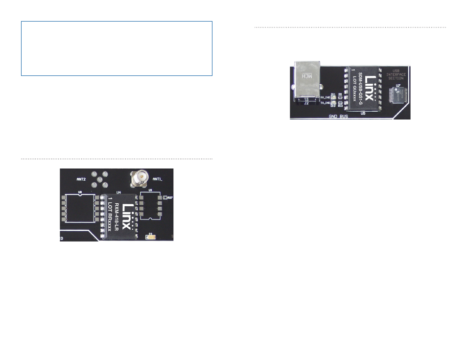
The Decoder Board RF Area
Figure 9 shows the RF area of the development board.
This board can be populated with either the LR Series receiver (as shown)
or the ES Series receiver. Both modules can be placed on the same pads
in the center of the section, but the ANT1 connector is populated for the
LR receiver and the ANT2 connector is populated for the ES receiver.
Figure 9: The Decoder Board RF Area
The Decoder Board USB Area
The decoder development board has a Linx SDM-USB-QS USB interface
module for use with the included development software. The module is
powered by the USB bus so does not pull any current from the battery.
Figure 10 shows this section.
The microcontroller on the right monitors the data lines and generates
commands that are sent to the development software on the PC via the
QS Series USB module. The RX_IND LED to the left of the module flashes
to indicate that data is being received from the PC, and the TX_IND line
flashes to indicate that the module is sending data to the PC.
Figure 10: The Decoder Board USB Area
Note:
The encoder board must be set to the same baud rate in order
for the signal to be received correctly. The maximum baud rate for the
LR Series is 10,000bps, so only 2,400 and 9,600bps can be used on
boards populated with these modules. The ES Series receiver can use
all four baud rates. If the switch is up, then the line is high, if it is down,
then the line is low.