Pin assignments, Pin descriptions, Module description – Linx Technologies SDM-USB-QS-S User Manual
Page 5: Theory of operation, Pin descriptions module description
– –
– –
4
5
Pin Assignments
Figure 5: SDM-USB-QS-S Pinout (Top View)
Pin Descriptions
Pin Number
Name
Description
1
USBDP
USB data signal plus
2
USBDM
USB data signal minus
3
GND
Ground supply
4
V
CC
Positive power supply
5
SUSP_IND
Goes low during USB Suspend Mode. This pin can be
used to power down external logic when the host puts
the USB bus into suspend mode.
6
RX_IND
This line will pulse low when receiving data from the USB
bus. This allows for the connection of a LED indicator.
7
TX_IND
This line will pulse low when transmitting data on the USB
bus. This allows for the connection of a LED indicator.
8
485_TX
Transmit enable line for RS-485 applications.
9
DTR
Data Terminal Ready control / handshake output
10
CTS
Clear to Send control / handshake input
11
RTS
Request To Send / handshake output
12
DATA_OUT
Transmit asynchronous data output
13
DATA_IN
Receive asynchronous data input
14
DSR
Data Set Ready control / handshake input
15
DCD
Data Carrier Detect control / input
16
RI
Ring Indicator control input
Figure 6: Pin Descriptions
USBDP
USBDM
GND
DSR
DATA_IN
DATA_OUT
RTS
CTS
DTR
TX_IND
VCC
SUSP_IND
RX_IND
485_TX
RI
DCD
1
2
3
4
5
6
7
8
9
10
11
12
13
14
15
16
Pin Descriptions
Module Description
The Linx SDM-USB-QS module converts USB signals from a host, such
as a PC or hub, into TTL logic level signals. This enables the module to
be connected directly to microcontrollers (or Linx RF modules for wireless
applications) or to RS-232 or RS-485 level converters for communication
with legacy devices. The module handles all complicated enumeration and
bus communication processes, freeing the designer to focus on handling
the data. All necessary firmware is included in the module and the device
descriptors can easily be changed to customize the module.
The host application software can access the USB device by simple,
custom functions or by standard Windows Win32 API calls. In addition,
Virtual COM Port drivers are available that make the USB module appear to
the PC as a COM port, without the need for additional system resources,
such as an IRQ or address. This allows the designer to program the
application software to use standard serial or parallel ports and then simply
select the port that represents the USB module. The drivers automatically
direct the data to the USB bus and the device.
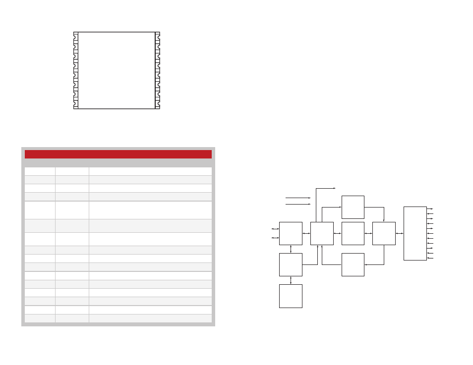
Theory of Operation
Figure 7 shows a block diagram of the QS module.
The USB transceiver block provides the physical interface for the USB
signalling.
Serial Interface
Engine (SIE)
USB Protocol
Engine
UART FIFO
Controller
USB
Transceiver
RX Buffer
384 Bytes
TX Buffer
128 Bytes
USB DPLL
Clock
SUSP_IND
USBDP
USBDM
DATA_OUT
DATA_IN
RTS
CTS
DTR
DSR
DCD
RI
485_TX
TX_IND
RX_IND
UART
VCC
GND
Figure 7: SDM-USB-QS-S Block Diagram