Normal mode – Altera MAX 10 Clocking and PLL User Manual
Page 22
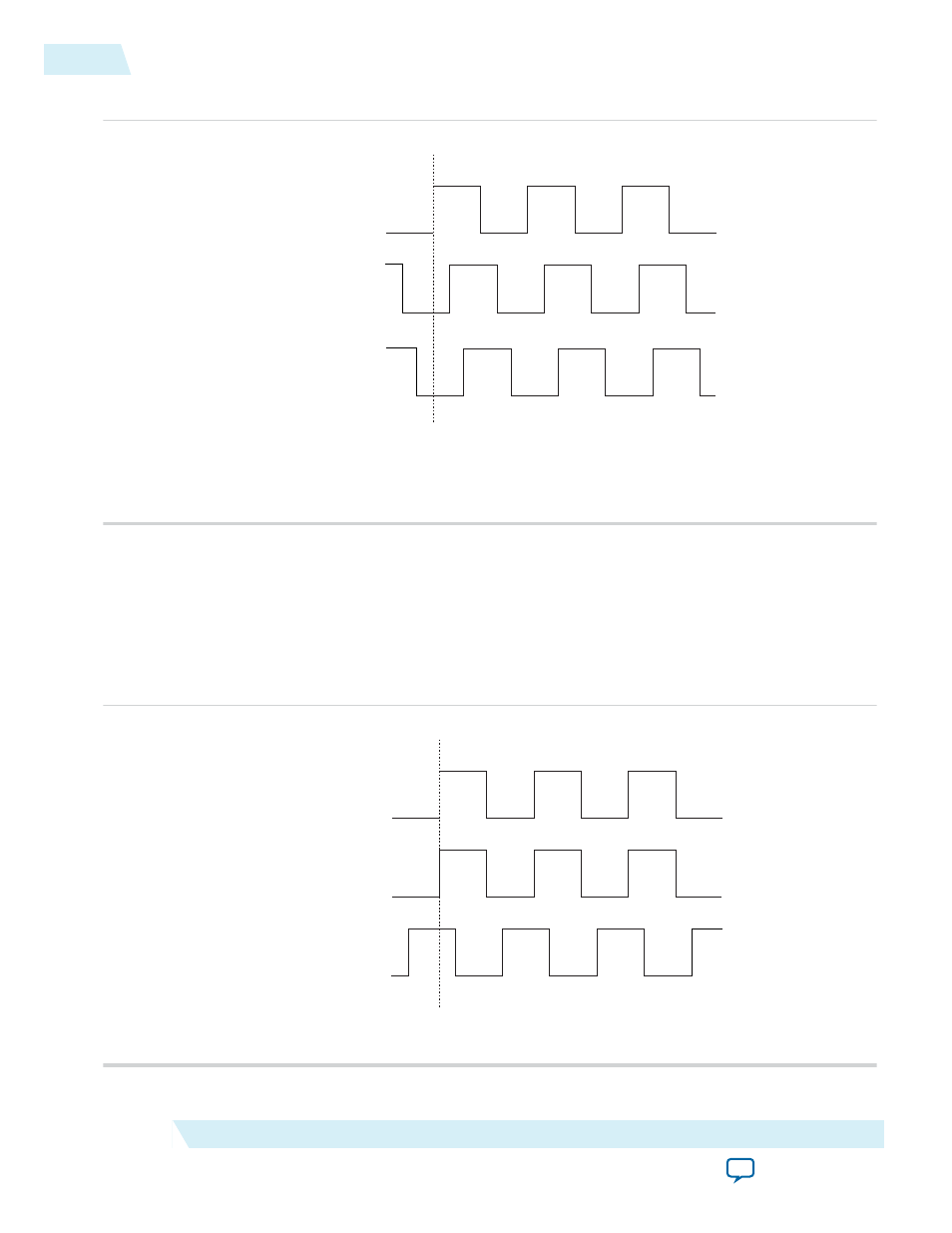
Figure 2-13: Example of Phase Relationship Between the PLL Clocks in No Compensation Mode
PLL Reference
Clock at the Input Pin
PLL Clock at the
Register Clock Port
(1), (2)
External PLL Clock
Outputs
(2)
Phase Aligned
Notes:
(1) Internal clocks fed by the PLL are phase-aligned to each other.
(2) The PLL clock outputs can lead or lag the PLL input clocks. The PLL clock outputs lag the
PLL input clocks depending on the routine delays.
Normal Mode
In normal mode, the PLL fully compensates the delay introduced by the GCLK network. An internal clock
in normal mode is phase-aligned to the input clock pin. In this mode, the external clock output pin has a
phase delay relative to the input clock pin. The Quartus II software timing analyzer reports any phase
difference between the two.
Figure 2-14: Example of Phase Relationship Between the PLL Clocks in Normal Compensation Mode
PLL Reference
Clock at the Input pin
PLL Clock at the
Register Clock Port
External PLL Clock
Outputs
(1)
Phase Aligned
Note:
(1) The external clock output can lead or lag the PLL internal clock signals.
2-16
Normal Mode
UG-M10CLKPLL
2015.05.04
Altera Corporation
MAX 10 Clocking and PLL Architecture and Features