Programming internal flash memory, Clock circuitry, General-purpose clock – Altera MAX 10 FPGA User Manual
Page 18: Programming internal flash memory –6, Clock circuitry –6, General-purpose clock –6
3–6
Chapter 3: Board Components
Clock Circuitry
MAX 10 FPGA (10M08S, 144-EQFP) Evaluation Kit
October 2014
Altera Corporation
User Guide
Programming Internal Flash Memory
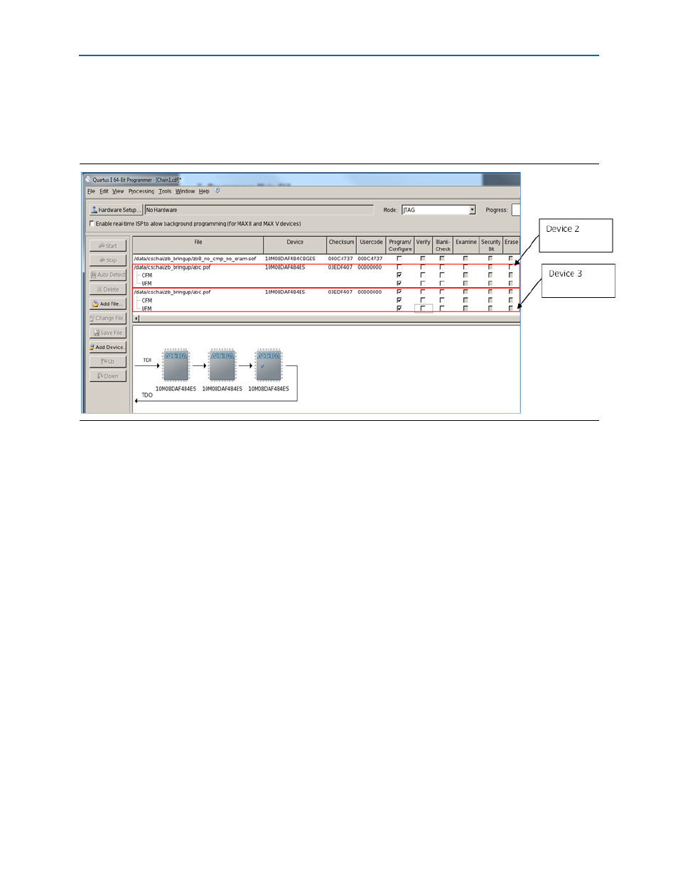
After generating the .pof file, Quartus II Programmer can be used to program the
internal flash memory through JTAG connection. The following shows an example of
the Quartus II Programmer.
There are 2 scenarios when using the Quartus II Programmer to program a .pof file
into MAX 10 devices:
1. For Device 2, the Programmer will just erase and configure CFM and UFM sector
in the internal flash memory, but the ICB setting will be preserved. However,
before starting the programming, the makes sure the ICB setting in the device and
the ICB setting in the .pof file are the same. If both ICB settings are different, the
Programmer still erases and programs the full internal memory including the ICB
setting, even though only CFM and UFM are selected in the Programmer.
2. For Device 3, the Programmer will erase and program full internal memory, which
includes the ICB setting, CFM, and UFM.
Before enabling real-time ISP for internal flash memory programming, you need to
ensure the MAX 10 FPGA is in user mode, otherwise the programming process will
fail.
Clock Circuitry
General-Purpose Clock
One general-purpose clock is provided to the FPGA global clock inputs for general
FPGA design. The clock source is from the following component:
■
A 50-MHz oscillator to the clock input CLK0p of bank 2.
Figure 3–2. Quartus II Programmer