General user input/output, User-defined dip switch, General user input/output –8 – Altera MAX 10 FPGA User Manual
Page 20: User-defined dip switch –8
3–8
Chapter 3: Board Components
General User Input/Output
MAX 10 FPGA (10M08S, 144-EQFP) Evaluation Kit
October 2014
Altera Corporation
User Guide
General User Input/Output
This section describes the user I/O interface to the FPGA:
■
User-defined DIP switch
■
User-defined LEDs
User-Defined DIP Switch
Board reference SW3 is a 6-pin DIP switch. Switches 1 through 5 are user-defined, and
provide additional FPGA input control. When the switch is in the OPEN or ON
position, a logic 1 is selected. When the switch is in the CLOSED or OFF position, a
logic 0 is selected. There is no board-specific function for these switches.
Table 3–4
lists the user-defined DIP switch schematic signal names and their
corresponding MAX 10 FPGA pin numbers.
J4.6
ARDUINO_A5
12
Arduino analog channel input through the op-amp
filter circuit to the FPGA ADC IP input channel
ADC1IN6
J4.7
ARDUINO_A6
13
Arduino analog channel input through the op-amp
filter circuit to the FPGA ADC IP input channel
ADC1IN7
J4.8
ARDUINO_A7
14
Arduino analog channel input through the op-amp
filter circuit to the FPGA ADC IP input channel
ADC1IN8
J5.1
ARDUINO_IO7
86
Arduino digital I/O input to FPGA
J5.2
ARDUINO_IO6
84
Arduino digital I/O input to FPGA
J5.3
ARDUINO_IO5
81
Arduino digital I/O input to FPGA
J5.4
ARDUINO_IO4
79
Arduino digital I/O input to FPGA
J5.5
ARDUINO_IO3
77
Arduino digital I/O input to FPGA
J5.6
ARDUINO_IO2
76
Arduino digital I/O input to FPGA
J5.7
ARDUINO_IO1
75
Arduino digital I/O input to FPGA
J5.8
ARDUINO_IO0
74
Arduino digital I/O input to FPGA
Table 3–3. Arduino Connector Pin Assignments, Signal Names and Functions (Part 2 of 2)
Board
Reference
Schematic Signal Name
MAX 10 FPGA
Device Pin Number
Description
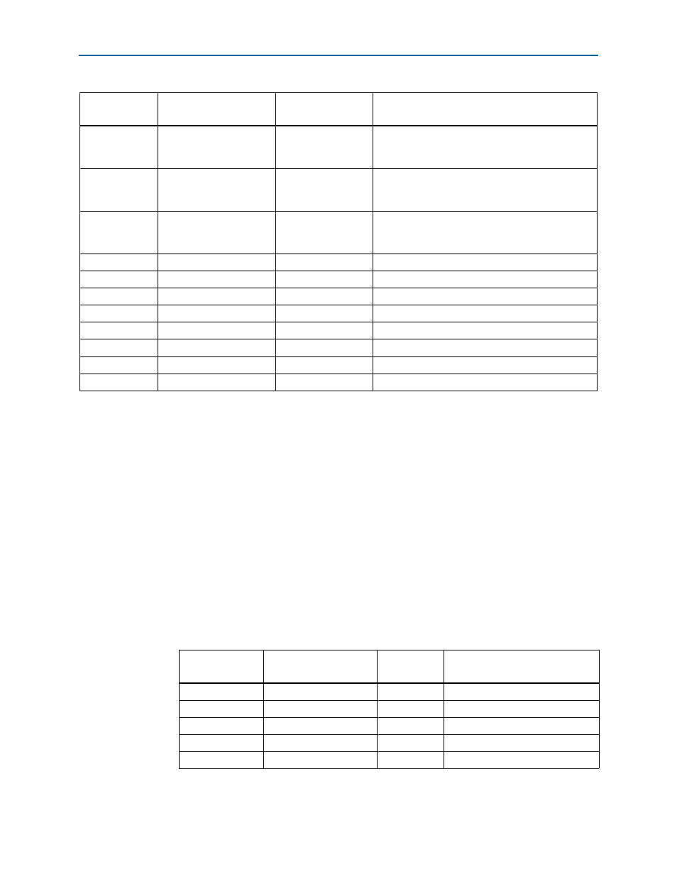
Table 3–4. User-Defined DIP Switch Schematic Signal Names and Functions
Board Reference
SW3
Schematic Signal Name
I/O Standard
MAX 10 FPGA Device Pin Number
1
Switch 1
3.3-V
120
2
Switch 2
3.3-V
124
3
Switch 3
3.3-V
127
4
Switch 4
3.3-V
130
5
Switch 5
3.3-V
131