Factory default switch settings, Factory default switch settings –2 – Altera Cyclone V GX FPGA User Manual
Page 12
4–2
Chapter 4: Development Board Setup
Factory Default Switch Settings
Cyclone V GX FPGA Development Kit
October 2012
Altera Corporation
User Guide
f
For more information about the PFL megafunction, refer to
.
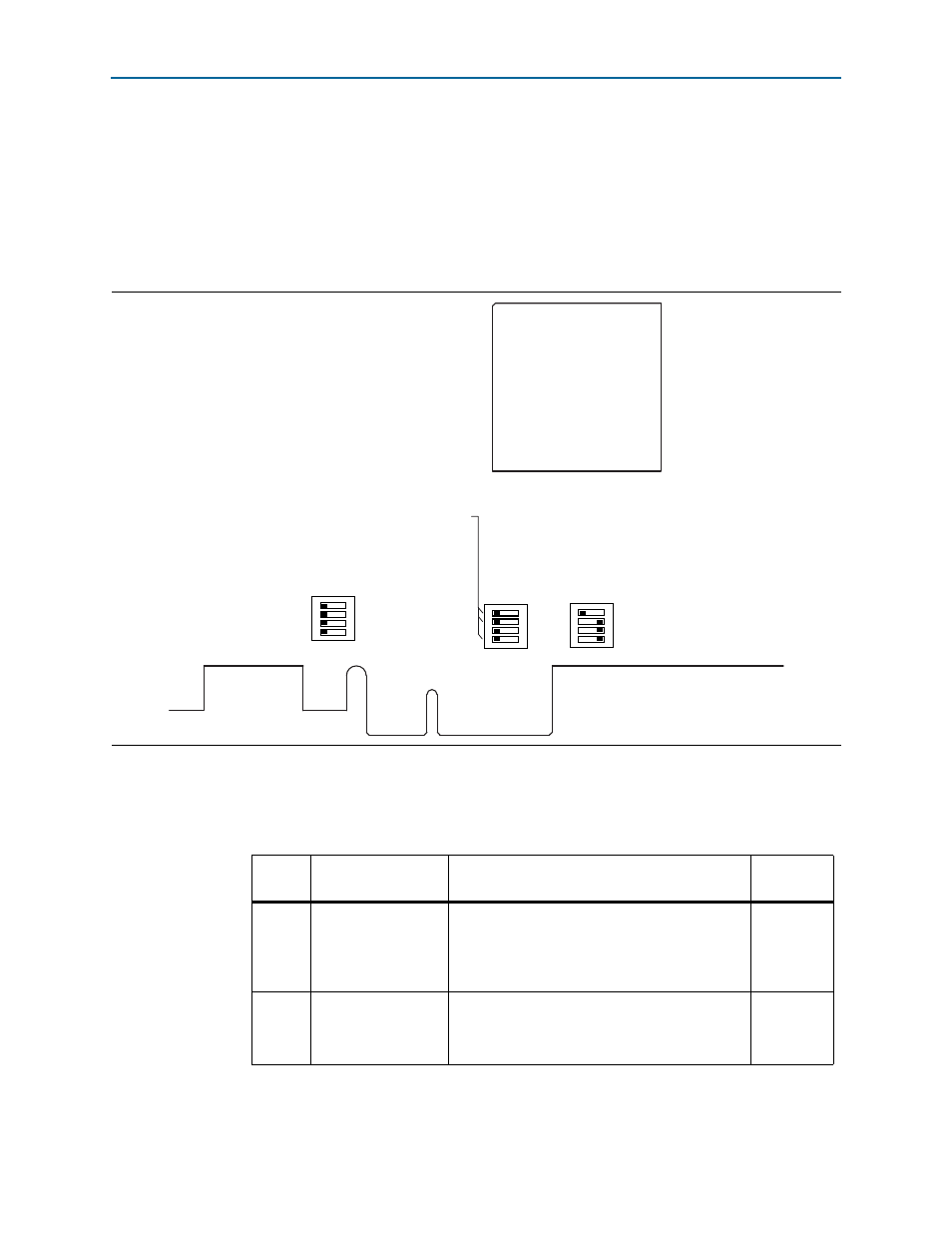
Factory Default Switch Settings
This section shows the factory switch settings (
) for the Cyclone V GX
FPGA development board.
To restore the switches to their factory default settings, perform these steps:
1. Set the DIP switch bank (SW3) to match
and
.
Figure 4–1. Switch Locations and Default Settings
SW3
CLK SEL
CLK EN
FACT LOAD
SEC MODE
PCIE_PRSNT2n_x1
PCIE_PRSNT2n_x4
-
FAN_FORCE_ON
SW5
5M2210_JTAG_EN
HSMA_JTAG_EN
PCIE_JTAG_EN
-
SW4
On
Off
On
Off
On
Off
ON
ON
ON
Table 4–1. SW3 DIP Switch Settings (Part 1 of 2)
Switch
Board
Label
Function
Default
Position
1
CLK SEL
Switch 1 has the following options:
■
On (0) = SMA input clock is selected.
■
Off (1) = Programmable oscillator clock is
selected.
Off
2
CLK EN
Switch 2 has the following options:
■
On (0) = On-board oscillator is disabled.
■
Off (1) = On-board oscillator is enabled.
Off