Feffective – Altera Device-Specific Power Delivery Network User Manual
Page 8
1–4
Chapter 1: User Guide for the Device-Specific Power Delivery Network (PDN) Tool
PDN Decoupling Methodology Review
Device-Specific Power Delivery Network (PDN) Tool User Guide
September 2012
Altera Corporation
■
The maximum allowable AC ripple on the power rail as a percentage of the supply
voltage. The maximum allowable AC ripple varies for different power rails. For
information about the recommended maximum allowable AC ripple for power
rails, refer to the table in the Introduction tab of the PDN tool.
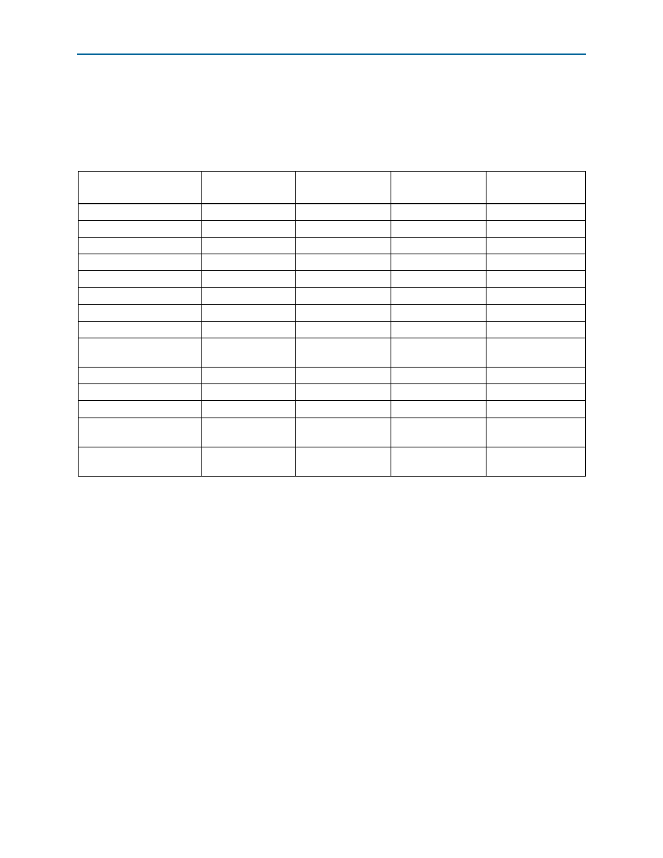
Table 1–1 on
page 1–4
shows ripple information for the power rails of Stratix IV GX device.
F
EFFECTIVE
As shown in
, a capacitor reduces PDN impedance by
providing a least-impedance route between power and ground. Impedance of a
capacitor at high frequency is determined by its parasitics (ESL and ESR). For a
PCB-mount capacitor, the parasitics include not only the parasitic from the capacitors
themselves but also the parasitics associated with mounting, PCB spreading, and
packaging. Therefore, PCB capacitor parasitics are generally higher than those of
on-package decoupling capacitor and on-die-capacitance. Decoupling using PCB
capacitors becomes ineffective at high frequency. Using PCB capacitors for PDN
decoupling beyond their effective frequency range brings little improvement to PDN
performance and raises the bill of materials (BOM) cost.
To help reduce over-design of PCB decoupling, this release of the PDN tool provides a
suggested PCB decoupling design cut-off frequency (F
EFFECTIVE
) as another guideline.
It is calculated using the PCB, package, and die parasitics. You only need to design
PCB decoupling that keeps Z
EFF
under Z
TARGET
up to F
EFFECTIVE
.
Table 1–1. Settings for the Stratix IV GX Device Power Rails
Rail Name
Voltage (V)
Allowable Ripple
Percentage (±)
Transient Current
Percentage (%)
Notes
VCC
0.9 V
5%
50%
Core
VCCIO
1.2 V - 3.0 V
5%
50%
I/O Bank
VCCPD
2.5 V
5%
50%
I/O Pre-Drivers
VCCA_PLL
2.5 V
3%
20%
PLL (Analog)
VCCD_PLL
0.9 V
3%
20%
PLL (Digital)
VCC_CLKIN
2.5 V
5%
50%
Diff Clock Input
VCCR
1.1 V
3%
30%
XCVR RX (Analog)
VCCT
1.1 V
3%
30%
XCVR TX (Analog)
VCCA
3.0 V
5%
10%
XCVR High Voltage
Power
VCCH_GXB
1.5 V
3%
10%
XCVR I/O Buffer Block
VCCL_GXB
1.1 V
3%
20%
XCVR Clock Block
VCCHIP
0.9 V
5%
50%
PCIE Hard IP (Digital)
VCCPT
1.5 V
3%
20%
Programmable Power
Tech
VCCAUX
2.5 V
3%
20%
Programmable Power
Tech Aux
Note to
Table 1–1
:
(1) For more information about power rail functions, refer to the pin connection guidelines for the selected device family.