Altera Arria V GT FPGA Development Board User Manual
Page 19
Chapter 2: Board Components
2–9
MAX II CPLD EPM2210 System Controller
December 2014
Altera Corporation
Arria V GT FPGA Development Board
Reference Manual
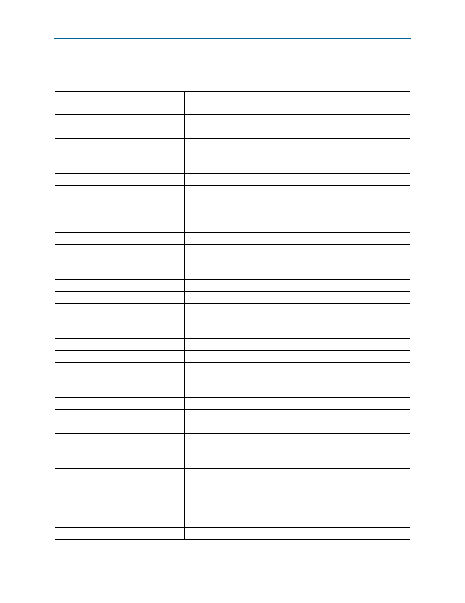
lists the I/O signals present on the MAX
II CPLD EPM2210 System
Controller. The signal names and functions are relative to the MAX
II device (U2).
Table 2–5. MAX II CPLD EPM2210 System Controller Device Pin-Out (Part 1 of 5)
Schematic Signal Name
MAX II CPLD
Pin Number
I/O Standard
Description
CLK125A_EN
B13
2.5-V
125 MHz oscillator enable
CLK125B_EN
D7
2.5-V
125 MHz oscillator enable
CLK50_EN
D11
2.5-V
50 MHz oscillator enable
CLK_CONFIG
K6
2.5-V
100 MHz configuration clock input
CLK_ENABLE
B5
2.5-V
DIP switch for clock oscillator enable
CLK_SEL
E7
2.5-V
DIP switch for clock select—SMA or oscillator
CLKIN_MAX_50
K13
2.5-V
50 MHz clock input
CLOCK_SCL
C14
2.5-V
Programmable oscillator I
2
C clock
CLOCK_SDA
L4
2.5-V
Programmable oscillator I
2
C data
CPU1_RESETN
B8
2.5-V
FPGA 1 reset push button
CPU2_RESETN
E6
2.5-V
FPGA 2 reset push button
DEVICE1_LED
D13
2.5-V
FPGA 1 configuration done LED
DEVICE2_LED
C15
2.5-V
FPGA 2 configuration done LED
EXTRA_SIG0
B10
2.5-V
Reserved for future use.
EXTRA_SIG1
F16
1.8-V
Reserved for future use.
EXTRA_SIG2
J16
1.8-V
Reserved for future use.
FACTORY_USER1
A5
2.5-V
Load factory or user design at power-up
FACTORY_USER2
C4
2.5-V
Load factory or user design at power-up
FACTORY_REQUEST
B9
2.5-V
On-Board USB-Blaster II request to send FACTORY command
FACTORY_STATUS
F10
2.5-V
On-Board USB-Blaster II FACTORY command status
FLASH_ACCESSN
B12
1.8-V
FM bus flash memory access indication
FLASH_ADVN
G15
1.8-V
FM bus flash memory address valid
FLASH_CEN
E16
1.8-V
FM bus flash memory chip enable
FLASH_CLK
E17
1.8-V
FM bus flash memory clock
FLASH_OEN
F14
1.8-V
FM bus flash memory output enable
FLASH_RDYBSYN
D18
1.8-V
FM bus flash memory ready
FLASH_RESETN
F13
1.8-V
FM bus flash memory reset
FLASH_WEN
D17
1.8-V
FM bus flash memory write enable
FM_A0
T17
1.8-V
FM bus address
FM_A1
R15
1.8-V
FM bus address
FM_A2
T16
1.8-V
FM bus address
FM_A3
F15
1.8-V
FM bus address
FM_A4
R16
1.8-V
FM bus address
FM_A5
P15
1.8-V
FM bus address
FM_A6
R17
1.8-V
FM bus address
FM_A7
P14
1.8-V
FM bus address