Fmc connector, Fmc connector –46 – Altera Arria V GT FPGA Development Board User Manual
Page 56
2–46
Chapter 2: Board Components
Components and Interfaces
Arria V GT FPGA Development Board
December 2014
Altera Corporation
Reference Manual
FMC Connector
The development board contains a high pin count (HPC) FPGA mezzanine card
(FMC) connector that functions with a quadrature amplitude modulation (QAM)
digital-to-analog converter (DAC) FMC module or daughter card. This pinout
satisfies a QAM DAC that requires 58 LVDS data output pairs, one LVDS input clock
pair, and three low-voltage differential signaling (LVDS) control pairs from the Arria
V. These pins also have the option to be used as single-ended I/O pins. The VCCIO
supply for the FMC A banks in the low pin count (LPC) and HPC provide a variable
voltage of 1.5 V, 1.8 V, 2.5 V (default), or 3.3 V. The VCCIO supply for the FMC B bank
in the HPC provides a variable voltage from 1.2 V to 3.3 V, which can be supplied by
the FMC module. However, for the sake of device safety concerns, a jumper is
available for you to connect this bank to the same VCCIO used for the FMC A banks.
This allows the VCCIO pins on the FPGA to be tied to a known power. The VCCIO
pins also allows you the option to perform a manual check for the module’s input
voltage before connecting to the FPGA. This is to ensure that the module does not
exceed the power supply maximum voltage rating.
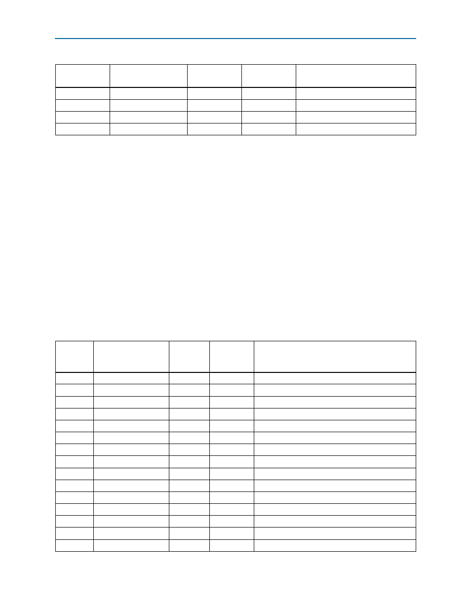
lists the FMC connector pin assignments, signal names, and functions.
19
SFP_TX_N2
J36
3.3-V LVTTL
Transmitter data
18
SFP_TX_P2
J37
3.3-V LVTTL
Transmitter data
7
SFP_TX_RS02
AP14
3.3-V LVTTL
Reserved
9
SFP_TX_RS12
AN7
3.3-V LVTTL
Reserved
Table 2–28. SFP+ Modules Pin Assignments, Schematic Signal Names, and Functions (Part 2 of 2)
Board
Reference
Schematic
Signal Name
Arria V GT FPGA
Pin Number
I/O Standard
Description
Table 2–29. FMC Connector Pin Assignments, Schematic Signal Names, and Functions (Part 1 of 7)
Board
Reference
(J10)
Schematic
Signal Name
Arria V GT
FPGA
Pin Number
I/O Standard
Description
D1
FMC_C2M_PG
—
2.5-V CMOS
Power good output
K4
FMC_CLK_BIDIR_P2
AE23
2.5-V CMOS
Clock input or output 2
K5
FMC_CLK_BIDIR_N2
AD22
2.5-V CMOS
Clock input or output 2
J2
FMC_CLK_BIDIR_P3
AU22
2.5-V CMOS
Clock input or output 3
J3
FMC_CLK_BIDIR_N3
AT22
2.5-V CMOS
Clock input or output 3
B1
FMC_CLK_DIR
AW21
2.5-V CMOS
Clock direction select for FMC_CLK_BIDIR
H4
FMC_CLK_M2C_P0
AV19
2.5-V CMOS
Clock input 0
H5
FMC_CLK_M2C_N0
AU19
2.5-V CMOS
Clock input 0
G2
FMC_CLK_M2C_P1
AF21
2.5-V CMOS
Clock input 1
G3
FMC_CLK_M2C_N1
AE21
2.5-V CMOS
Clock input 1
C3
FMC_DP_C2M_N0
AD4
2.5-V CMOS
Transmit channel
A23
FMC_DP_C2M_N1
Y4
2.5-V CMOS
Transmit channel
A27
FMC_DP_C2M_N2
T4
2.5-V CMOS
Transmit channel
A31
FMC_DP_C2M_N3
P4
2.5-V CMOS
Transmit channel
A35
FMC_DP_C2M_N4
H4
2.5-V CMOS
Transmit channel