Hsmc connector (j1), Hsmc connector (j1) –4 – Altera Santa Cruz User Manual
Page 10
2–4
Chapter 2: Board Components
HSMC Connector (J1)
Santa Cruz, USB, MICTOR, SD Card HSMC Reference Manual
© December 2008 Altera Corporation
HSMC Connector (J1)
The THDB-SUM board contains an Altera standard HSMC connector (J1) to connect
to Altera FPGA starter or development board. All the other connector interfaces on
the THDB-SUM board are connected to the HSMC connector.
show the pin-outs of the HSMC connector for
banks 1, 2, and 3, respectively.
JP4
SC connector logic level configuration
header
When open, selects 3.3 V for Santa Cruz header I/O voltage.
When closed, selects 5.0 V.
U1–U2
Bus switches
Multiplexer to switch between USB or Santa Cruz I/O based
on setting of JP2.
U3–U8
Level shifters
Provides I/O level shifting based on jumper settings of JP3
and JP4.
U10
I
2
C serial EEPROM
Uses one 2-Kbit EEPROM.
U11
USB On-The-Go transceiver
Provide USB interface to the HSMC interface host board.
Table 2–1. THDB-SUM Board (Part 2 of 2)
Board Reference
Name
Description
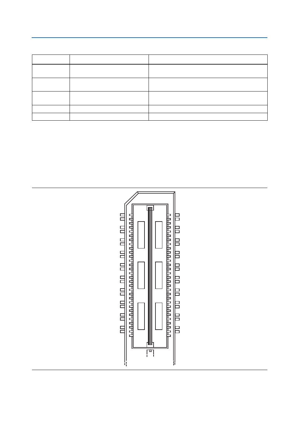
Figure 2–3. HSMC Connector Bank 1 Pin-Outs
NC
2
4
6
8
10
12
14
16
18
20
22
24
26
28
30
32
34
36
38
40
1
3
5
7
9
11
13
15
17
19
21
23
25
27
29
31
33
35
37
39
NC
NC
NC
NC
NC
NC
NC
NC
NC
NC
NC
NC
NC
NC
NC
HSMC_SCL
HSMC_TMS
HSMC_TDI
SD_WPn
NC
NC
NC
NC
NC
NC
NC
NC
NC
NC
NC
NC
NC
NC
NC
HSMC_SDA
HSMC_TCK
HSMC_TDO
SD_DAT1
NC