NEXCOM NSA 5150 User Manual
Page 45
Copyright © 2013 NEXCOM International Co., Ltd. All Rights Reserved.
31
NSA 5150 User Manual
Chapter 2: Jumpers and Connectors
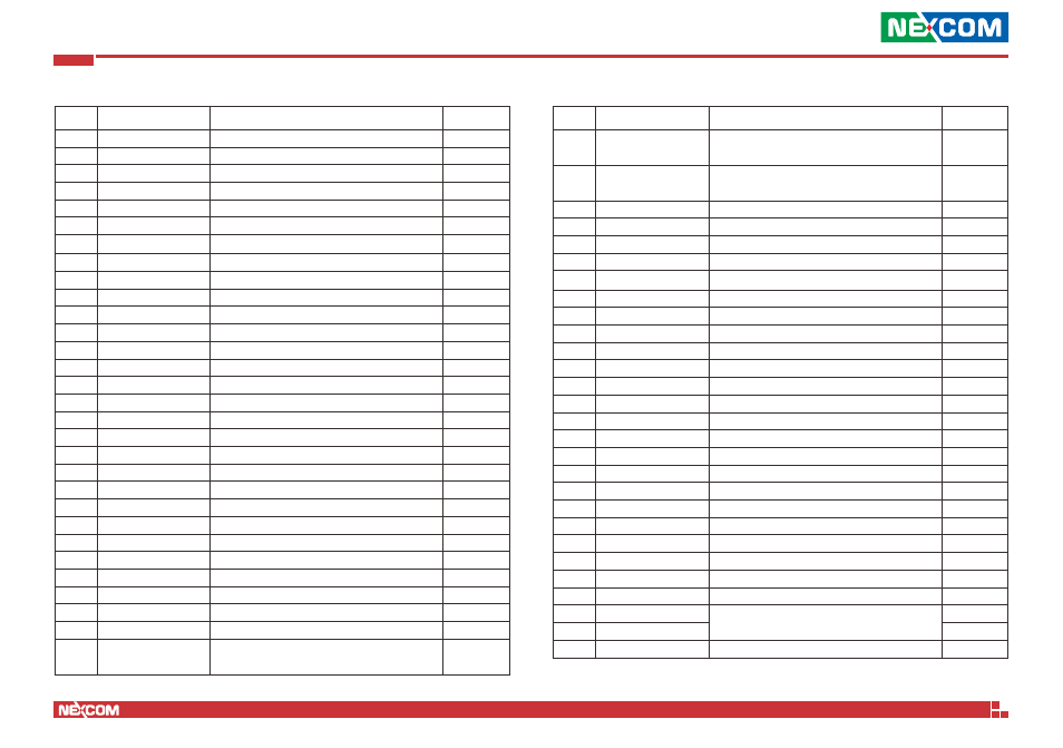
Pin
Definition
Pin
Direction
B1
GND
GND
B2
PCIE1_SEL1
High level (3.3VSB) (Identify for module)
O
B3
PCIE1_SEL2
Low level (GND) (Identify for module)
O
B4
PCIE1_SEL3
Low level (GND) (Identify for module)
O
B5
GND
GND
B6
GND
GND
B7
GND
GND
B8
PCIE1_SUSCLK
32KHz Clock output
O
B9
P3V3_DUAL
3.3VSB
Power
B10
P3V3_DUAL
3.3VSB
Power
B11
P3V3_DUAL
3.3VSB
Power
B12
P5V
5V
Power
B13
P5V
5V
Power
B14
P5V
5V
Power
B15
P5V
5V
Power
B16
P5V
5V
Power
B17
P3V3
3.3V
Power
B18
P3V3
3.3V
Power
B19
P3V3
3.3V
Power
B20
P3V3
3.3V
Power
B21
P3V3
3.3V
Power
B22
P3V3
3.3V
Power
B23
P3V3
3.3V
Power
B24
P12V
12V
Power
B25
P12V
12V
Power
B26
P12V
12V
Power
B27
P12V
12V
Power
B28
P12V
12V
Power
B29
SMB_ALERT#
SMBus ALERT#
I
B30
PE_WAKE_N
PCI Express Device Wake Event signal
1K pull-high to 3VDual
I
Pin
Definition
Pin
Direction
B31
ATX_PWROK_A1
Power good signal from ATX power supply
8.2K pull-high to 5VDual
O
B32
ATX_PWROK_A2
Power good signal from ATX power supply
8.2K pull-high to 5VDual
O
B33
GND
GND
B34
USB_4P
Universal Serial Bus Port Differential signal
I/O
B35
USB_4N
Universal Serial Bus Port Differential signal
I/O
B36
USB_OC45#
USB device Over current Indicators
I
B37
GND
GND
B38
GND
GND
B39
GND
GND
B40
GND
GND
B41
GND
GND
B42
GND
GND
B43
GND
GND
B44
GND
GND
B45
GND
GND
B46
GND
GND
B47
GND
GND
B48
GND
GND
B49
GND
GND
B50
GND
GND
B51
GND
GND
B52
GND
GND
B53
GND
GND
B54
GND
GND
B55
GND
GND
B56
PEG0_RX3P
CPU Primary PCI Express Receive Differential
Pair
I
B57
PEG0_RX3N
I
B58
GND
GND