Chapter 3 – DFI CD905-B series User Manual
Page 22
www.dfi .com
Chapter 3 Hardware Installation
22
Chapter 3
Signal
Pin#
Pin Type
Pwr Rail /Tolerance
PU/PD
Description
PCI_AD0
C24
PCI_AD1
D22
PCI_AD2
C25
PCI_AD3
D23
PCI_AD4
C26
PCI_AD5
D24
PCI_AD6
C27
PCI_AD7
D25
PCI_AD8
C28
PCI_AD9
D27
PCI_AD10
C29
PCI_AD11
D28
PCI_AD12
C30
PCI_AD13
D29
PCI_AD14
C32
PCI_AD15
D30
PCI_AD16
D37
PCI_AD17
C39
PCI_AD18
D38
PCI_AD19
C40
PCI_AD20
D39
PCI_AD21
C42
PCI_AD22
D40
PCI_AD23
C43
PCI_AD24
D42
PCI_AD25
C45
PCI_AD26
D43
PCI_AD27
C46
PCI_AD28
D44
PCI_AD29
C47
PCI_AD30
D45
PCI_AD31
C48
PCI_C/BE0#
D26
PCI_C/BE1#
C33
PCI_C/BE2#
C38
PCI_C/BE3#
C44
PCI_DEVSEL#
C36
I/O CMOS
3.3V / 5V
PU 8.2k to 3.3V
PCI bus Device Select, active low.
PCI_FRAME#
D36
I/O CMOS
3.3V / 5V
PU 8.2k to 3.3V
PCI bus Frame control line, active low.
PCI_IRDY#
C37
I/O CMOS
3.3V / 5V
PU 8.2k to 3.3V
PCI bus Initiator Ready control line, active low.
PCI_TRDY#
D35
I/O CMOS
3.3V / 5V
PU 8.2k to 3.3V
PCI bus Target Ready control line, active low.
PCI_STOP#
D34
I/O CMOS
3.3V / 5V
PU 8.2k to 3.3V
PCI bus STOP control line, active low, driven by cycle initiator.
PCI_PAR
D32
I/O CMOS
3.3V / 5V
PCI bus parity
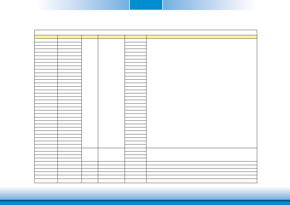
PCI Signals Descriptions
I/O CMOS
3.3V / 5V
PCI bus multiplexed address and data lines
I/O CMOS
3.3V / 5V
PCI bus byte enable lines, active low