Chapter 3 – DFI CD905-B series User Manual
Page 26
www.dfi .com
Chapter 3 Hardware Installation
26
Chapter 3
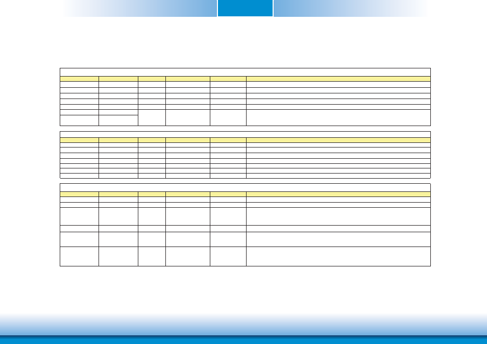
Signal
Pin#
Pin Type
Pwr Rail /Tolerance
PU/PD
Description
SPI_CS#
B97
O CMOS
3.3V Suspend/3.3V
Chip select for Carrier Board SPI - may be sourced from chipset SPI0 or SPI1
SPI_MISO
A92
I CMOS
3.3V Suspend/3.3V
Data in to Module from Carrier SPI
SPI_MOSI
A95
O CMOS
3.3V Suspend/3.3V
Data out from Module to Carrier SPI
SPI_CLK
A94
O CMOS
3.3V Suspend/3.3V
Clock from Module to Carrier SPI
SPI_POWER
A91
O
3.3V Suspend/3.3V
Power supply for Carrier Board SPI – sourced from Module – nominally
BIOS_DIS0#
A34
BIOS_DIS1#
B88
Signal
Pin#
Pin Type
Pwr Rail /Tolerance
PU/PD
Description
VGA_RED
B89
O Analog
Analog
PD 150R
Red for monitor. Analog output
VGA_GRN
B91
O Analog
Analog
PD 150R
Green for monitor. Analog output
VGA_BLU
B92
O Analog
Analog
PD 150R
Blue for monitor. Analog output
VGA_HSYNC
B93
O CMOS
3.3V / 3.3V
Horizontal sync output to VGA monitor
VGA_VSYNC
B94
O CMOS
3.3V / 3.3V
Vertical sync output to VGA monitor
VGA_I2C_CK
B95
I/O OD CMOS 3.3V / 3.3V
PU 2.2K to 3.3V
DDC clock line (I2C port dedicated to identify VGA monitor capabilities)
VGA_I2C_DAT
B96
I/O OD CMOS 3.3V / 3.3V
PU 2.2K to 3.3V
DDC data line.
Signal
Pin#
Pin Type
Pwr Rail /Tolerance
PU/PD
Description
I2C_CK
B33
I/O OD CMOS 3.3V Suspend/3.3V
PU 2.2K to 3.3VSB General purpose I2C port clock output
I2C_DAT
B34
I/O OD CMOS 3.3V Suspend/3.3V
PU 2.2K to 3.3VSB General purpose I2C port data I/O line
SPKR
B32
O CMOS
3.3V / 3.3V
Output for audio enunciator - the "speaker" in PC-AT systems.
This port provides the PC beep signal and is mostly intended for
debugging purposes.
WDT
B27
O CMOS
3.3V / 3.3V
Output indicating that a watchdog time-out event has occurred.
KBD_RST#
A86
I CMOS
3.3V / 3.3V
PU 10KW to 3.3V Input to Module from (optional) external keyboard controller that can force a reset. Pulled high on
the Module. This is a legacy artifact of the PC-AT.
KBD_A20GATE
A87
I CMOS
3.3V / 3.3V
PU 10KW to 3.3V Input to Module from (optional) external keyboard controller that can be used to control the CPU
A20 gate line. The A20GATE restricts the memory access to the bottom megabyte and is a legacy
artifact of the PC-AT.Pulled high on the Module.
VGA Signals Descriptions
Miscellaneous Signal Descriptions
SPI Signals Descriptions
I CMOS
NA
Selection straps to determine the BIOS boot device.
The Carrier should only float these or pull them low, please refer to
COM Express Module Base Specification Revision 2.1 for strapping options of BIOS disable signals.