Chapter 3 – DFI CD905-B2600 User Manual
Page 25
www.dfi .com
Chapter 3 Hardware Installation
25
Chapter 3
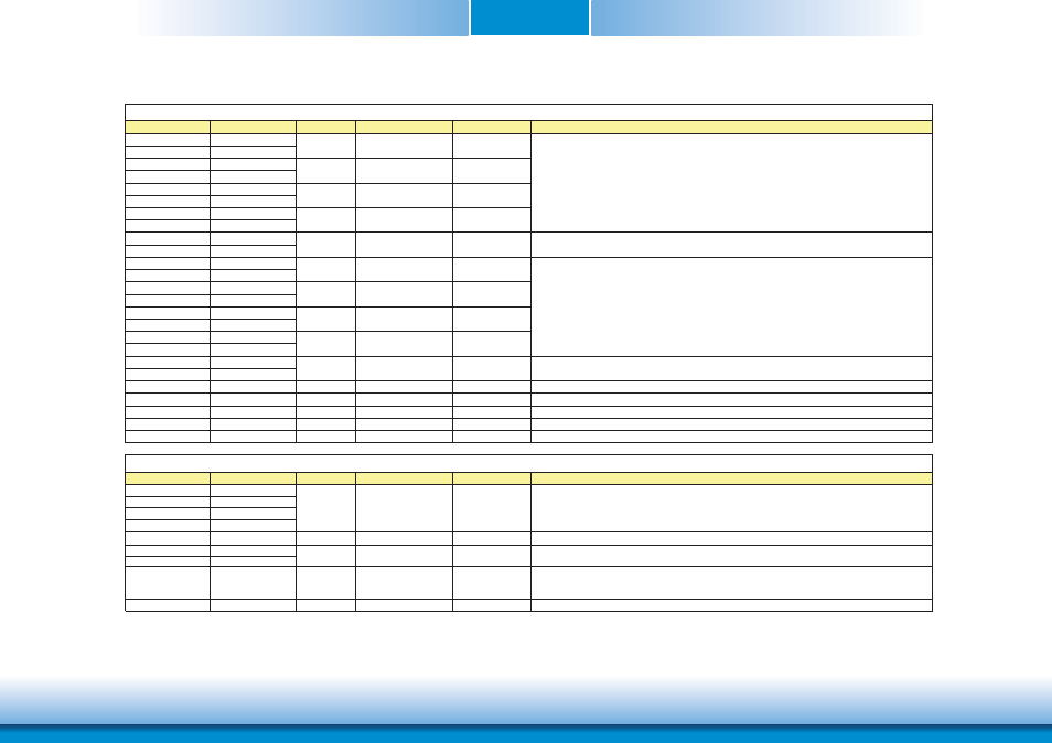
Signal
Pin#
Pin Type
Pwr Rail /Tolerance
PU/PD
Description
LVDS_A0+
A71
LVDS_A0-
A72
LVDS_A1+
A73
LVDS_A1-
A74
LVDS_A2+
A75
LVDS_A2-
A76
LVDS_A3+
A78
LVDS_A3-
A79
LVDS_A_CK+
A81
LVDS_A_CK-
A82
LVDS_B0+
B71
LVDS_B0-
B72
LVDS_B1+
B73
LVDS_B1-
B74
LVDS_B2+
B75
LVDS_B2-
B76
LVDS_B3+
B77
LVDS_B3-
B78
LVDS_B_CK+
B81
LVDS_B_CK-
B82
LVDS_VDD_EN
A77
O CMOS
3.3V / 3.3V
LVDS panel power enable
LVDS_BKLT_EN
B79
O CMOS
3.3V / 3.3V
LVDS panel backlight enable
LVDS_BKLT_CTRL B83
O CMOS
3.3V / 3.3V
LVDS panel backlight brightness control
LVDS_I2C_CK
A83
I/O OD
3.3V / 3.3V
I2C clock output for LVDS display use
LVDS_I2C_DAT
A84
I/O OD
3.3V / 3.3V
I2C data line for LVDS display use
Signal
Pin#
Pin Type
Pwr Rail /Tolerance
PU/PD
Description
LPC_AD0
B4
LPC_AD1
B5
LPC_AD2
B6
LPC_AD3
B7
LPC_FRAME#
B3
O CMOS
3.3V / 3.3V
LPC frame indicates the start of an LPC cycle
LPC_DRQ0#
B8
LPC_DRQ1#
B9
LPC_SERIRQ
A50
I/O CMOS
3.3V / 3.3V
PU 8.2k to 3.3V
LPC serial interrupt
LPC_CLK
B10
O CMOS
3.3V / 3.3V
PD 10K
LPC clock output - 33MHz nominal
I CMOS
3.3V / 3.3V
LPC serial DMA request
I/O CMOS
3.3V / 3.3V
LPC multiplexed address, command and data bus
LVDS Channel A differential clock
O LVDS
LVDS
LVDS Channel B differential pairs
O LVDS
LVDS
O LVDS
LVDS
O LVDS
LVDS
O LVDS
LVDS
O LVDS
LVDS
LVDS Channel B differential clock
LPC Signals Descriptions
LVDS Signals Descriptions
O LVDS
LVDS
LVDS Channel A differential pairs
O LVDS
LVDS
O LVDS
LVDS
O LVDS
LVDS