IBASE MI912 User Manual
Page 25
INSTALLATIONS
MI912 User’s Manual
21
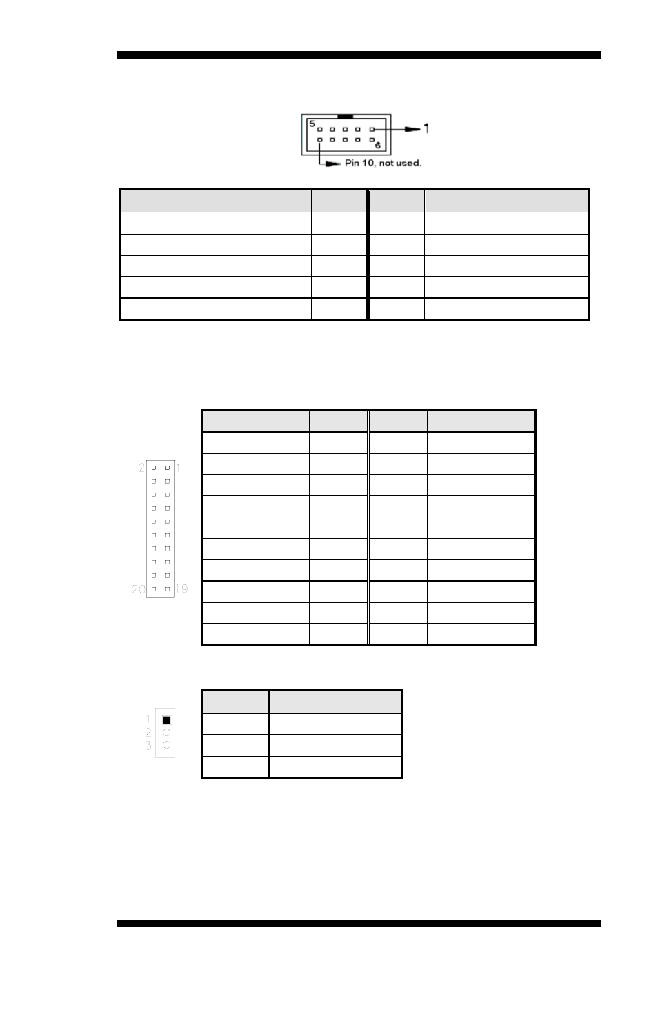
J2: COM2 Serial Port
COM2
Signal Name
Pin #
Pin #
Signal Name
DCD, Data carrier detect
1
6
DSR, Data set ready
RXD, Receive data
2
7
RTS, Request to send
TXD, Transmit data
3
8
CTS, Clear to send
DTR, Data terminal ready
4
9
RI, Ring indicator
GND, ground
5
10
Not Used
J3, J4: LVDS Connectors (1st channel, 2nd channel)
The LVDS connectors on board consist of the first channel (J3) and
second channel (J4).
Signal Name Pin #
Pin #
Signal Name
TX0-
2
1
TX0+
Ground
4
3
Ground
TX1-
6
5
TX1+
5V/3.3V
8
7
Ground
TX3-
10
9
TX3+
TX2-
12
11
TX2+
Ground
14
13
Ground
TXC-
16
15
TXC+
5V/3.3V
18
17
ENABKL
+12V
20
19
+12V
J5: LCD Backlight Connector
Pin #
Signal Name
1
+12V
2
Backlight Enable
3
Ground
J7: Mini PCI Connector
CN8, CN9: SATA Connectors