Connectors and jumpers list, Chapter 3, Board layout – Lanner LEC-3012 User Manual
Page 14
14
Board Layout
Chapter 3
Embedded and Industrial Computing
Connectors and Jumpers List
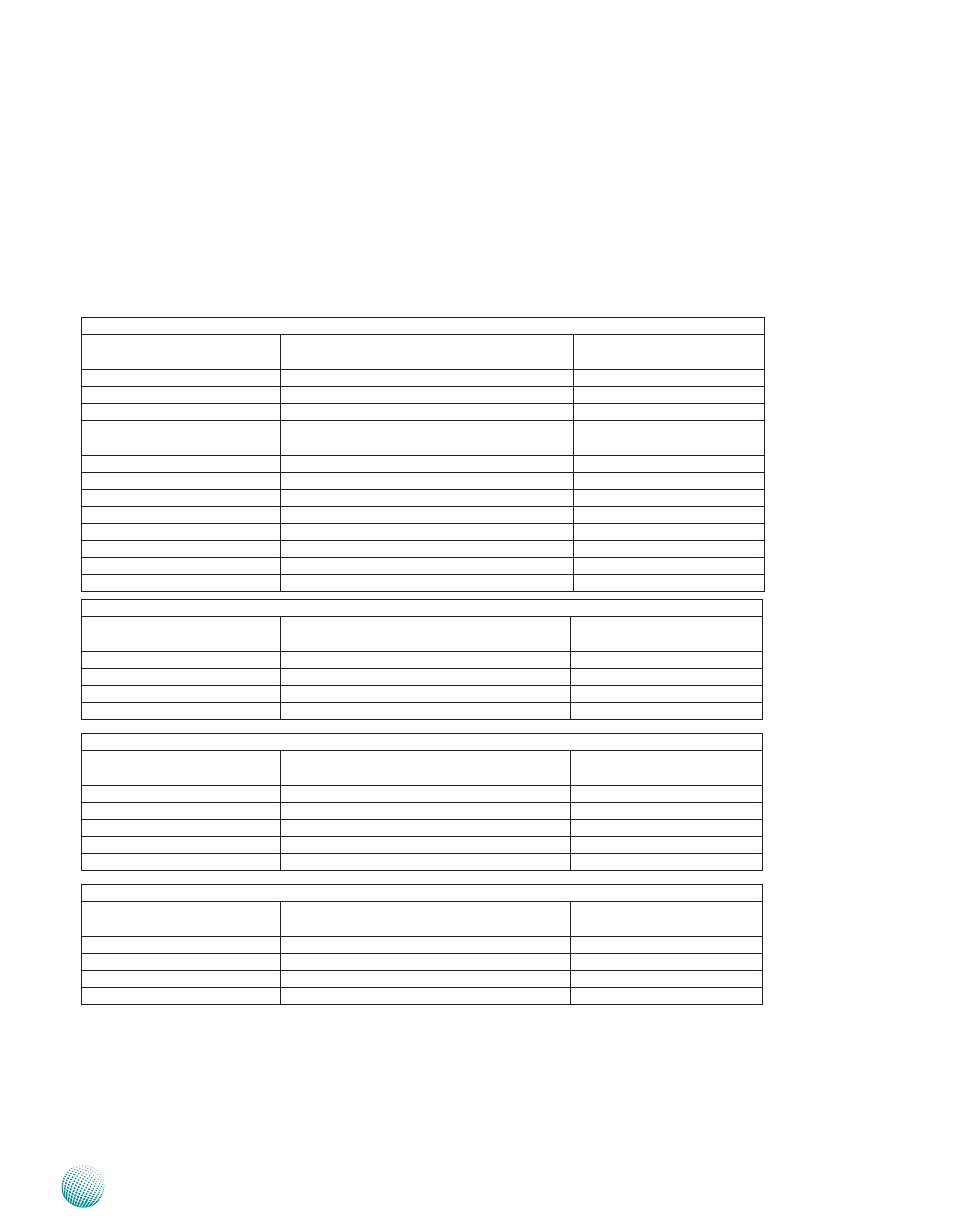
The tables below list the function of each of the board
jumpers and connectors by labels shown in the above
section. The next section in this chapter gives pin
definitions and instructions on setting jumpers.
Table 3.1 Connector List for LEB-3012
Labels
Function
Pin Definition Reference
Page
CN1
DC-in Connector
P15
CN2
CF Card Slot
P15
CN3
Dual USB Port
P15
J2
SMBus (System Management Bus) Communi-
cation Pin Header
Reserved for Factory Use
J3
SATA Connector
P15
J4
SATA Power Connector
P15
J5
SPI-ROM Header
Reserved for Factory Use
J6
Board to Board Connector
P16
JP1
Clear CMOS Pin Header
P16
RJ1/RJ2
LAN1/LAN2
P15
USB1
Additional USB Pin Header
P15
VGA1
VGA Port
P15
Table 3.2 Connector List for LEK-AU4
Labels
Function
Pin Definition Reference
Page
CN1
COM Port 1~4
P17
J1
SATA Connector
P17
J2
SATA Power Connector
P17
LAN3/LAN4
LAN3/LAN4
P18
Table 3.2 Connector List for LEK-AU6
Labels
Function
Pin Definition Reference
Page
CN1
COM Port 1~4
P17
CN2
COM Port 5~6
P18
J1
SATA Connector
P17
J2
SATA Power Connector
P17
LAN3/LAN4
LAN3/LAN4
P18
Table 3.2 Connector List for LEK-AU8
Labels
Function
Pin Definition Reference
Page
CN1
COM Port 1~4
P17
CN2
COM Port 5~8
P18
J1
SATA Connector
P17
J2
SATA Power Connector
P17