Chapter 3, Board layout – Lanner LEC-7105 User Manual
Page 14
14
Board Layout
Chapter 3
Embedded and Industrial Computing
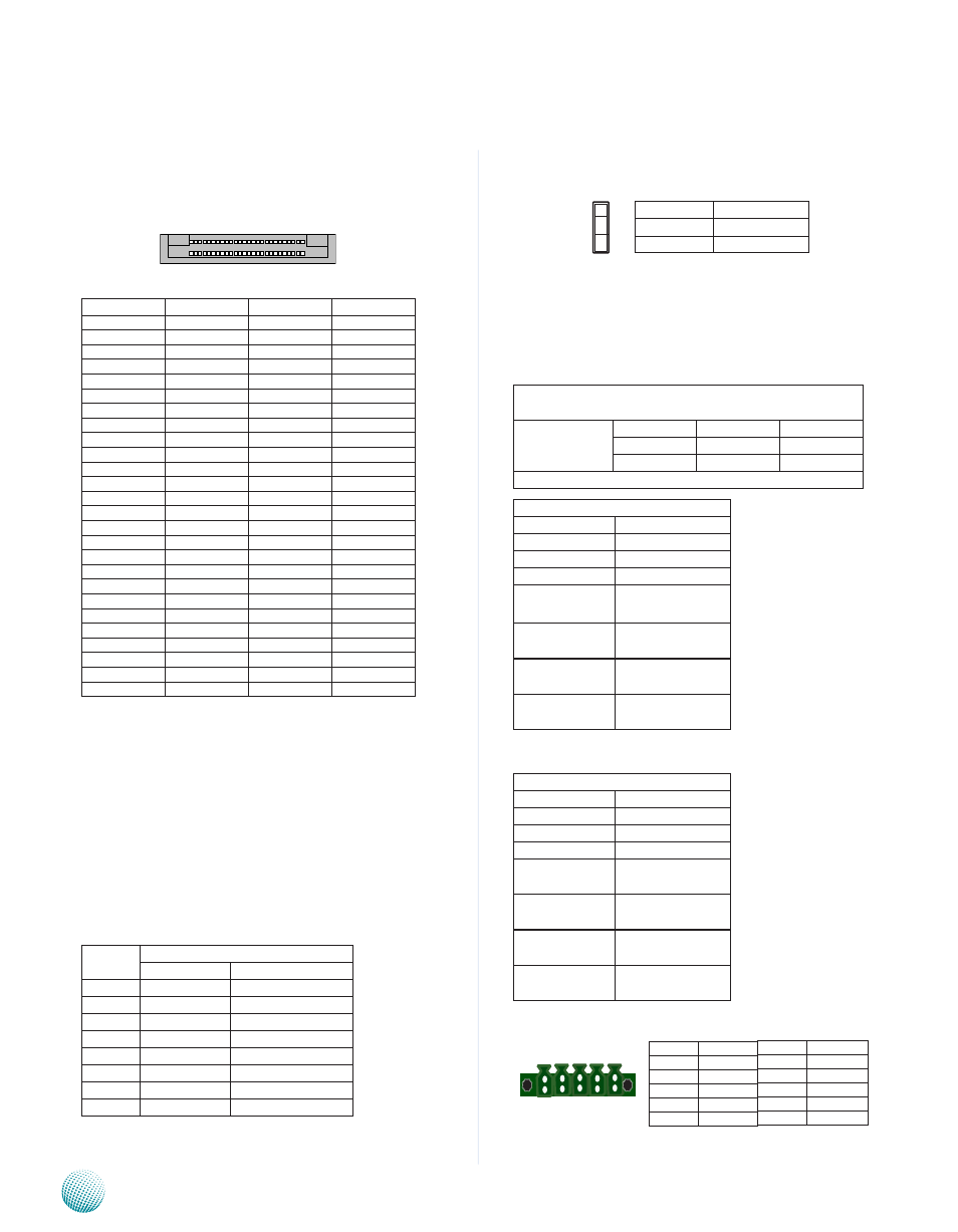
Clear CMOS jumper (JP3): It is for clearing the CMOS
memory.
Digital I/O (DIO1)
Digital IN/OUT(DIO1) Connector: The 8 pins of digital
Input/Output (GPIO) support input and output operations
through the 2x5-pin terminal block.
TTL Level is +5V; Maximum input/output current for
each port is 20mA
Input/Output Voltage
Logic
Register
0~2V
Low
0
2~5V
High
1
The output default value is 0
DIO Address LDN8
Address
Description
0x2e
SUPERIO_INDEX
0x2f
SUPERIO_DATA
0x07
BANK_REG
0xE6 (Bit 3)
GPO63
0: Low 1: High
0xE6 (Bit 2)
GPO62
0: Low 1: High
0xE6 (Bit 1)
GPO61
0: Low 1: High
0xE6 (Bit 0)
GPO60
0: Low 1: High
DIO Address LDN9
Address
Description
0x2e
SUPERIO_INDEX
0x2f
SUPERIO_DATA
0x07
BANK_REG
0xE6 (Bit 3)
GPI24
0: Low 1: High
0xE6 (Bit 2)
GPI25
0: Low 1: High
0xE6 (Bit 1)
GPI26
0: Low 1: High
0xE6 (Bit 0)
GPI27
0: Low 1:High
CompactFlash Connector (CFD1): It is for connecting a
Compact Flash card to be served as your system’s storage.
Pin No.
Function
Pin No.
Function
Pin
Signal
Pin
Signal
1
GNd
26
Cd1#
2
Pdd3
27
Pdd11
3
Pdd4
28
Pdd12
4
Pdd5
29
Pdd13
5
Pdd6
30
Pdd14
6
Pdd7
31
Pdd15
7
PdCS1_N
32
PdCS3_N
8
GNd
33
N/A
9
GNd
34
PdIOR_N
10
GNd
35
PdIOW_N
11
GNd
36
WE#
12
1GNd
37
IRQ14
13
VCC5
38
VCC5
14
GNd
39
CSEL#
15
GNd
40
N/A
16
GNd
41
PRST
17
GNd
42
PdIORdY
18
PdA2
43
PddREQ
19
PdA1
44
PddACK
20
PdA0
45
PdACTIVE
21
Pdd0
46
PATAdET
22
Pdd1
47
Pdd8
23
Pdd2
48
Pdd9
24
IOCS16#
49
Pdd10
25
Cd2#
50
GNd
LAN1/LAN2 Ports (LAN1/LAN2): The LAN ports are
provided by Realtek RTL8111E Ethernet Controllers. The
following lists its main features:
Wake-on-LAN and remote wake-up support
•
Microsoft NDIS5, NDIS6 Checksum Offload (IPv4, IPv6,
•
TCP, UDP) and Segmentation Task-offload (Large send
v1 and Large send v2) support
Supports IEEE 802.1P Layer 2 Priority Encoding
•
Supports IEEE 802.1Q VLAN tagging
•
Pin No. Description
Fast Ethernet Gigabit Ethernet
1
TX+
BI_DA+
2
TX-
BI_DA-
3
RX+
BI_DB+
4
--
BI_DC+
5
--
BI_DC-
6
RX-
BI_DB-
7
--
BI_DD+
8
--
BI_DD-
Pin No. Pin Name
1
Input0
3
Input1
5
Input2
7
Input3
9
GNd
Pin No. Pin Name
2
Output0
4
Output1
6
Output2
8
Output3
10
GNd
25 1
50 26
Pin No.
Pin Name
1-2
Normal (default)
2-3
Clear CMOS
1
2
3
1 3 5 7 9
2 4 6 8 10