Using the data line, Power supply requirements – Linx Technologies TRM-xxx-LT User Manual
Page 10
– –
– –
14
15
It is important to recognize that in many actual use environments, ambient
noise and interference may enter the receiver at levels well above the
squelch threshold. For this reason, it is always recommended that the
product’s protocol be structured to allow for the possibility of hashing, even
when an external squelch circuit is employed.
Power Supply Requirements
The module does not have an internal
voltage regulator; therefore it requires a
clean, well-regulated power source. While
it is preferable to power the unit from a
battery, it can also be operated from a
power supply as long as noise is less than
20mV. Power supply noise can affect the
transmitter modulation; therefore, providing
a clean power supply for the module should
be a high priority during design.
A 10
Ω resistor in series with the supply followed by a 10µF tantalum
capacitor from V
CC
to ground will help in cases where the quality of the
supply is poor. Note that the values may need to be adjusted depending on
the noise present on the supply line.
Using the Data Line
The CMOS-compatible DATA line is used for both the transmitter data and
the recovered receiver data. Its function is controlled by the state of the
T/R_ SEL line, so it is an input when in transmit mode and an output when
in receive mode. The output is normally connected to a transcoder IC or a
microprocessor for data encoding and decoding.
It is important to note that the transceiver does not provide hysteresis or
squelching of the DATA line when in receive mode. This means that, in the
absence of a valid transmission or transitional data, the DATA line switches
randomly. This noise can be handled in software by implementing a noise-
tolerant protocol as described in Linx Application Note AN-00160. If a
software solution is not appropriate, then the transceiver can be squelched.
Squelching disables the DATA output when the RSSI voltage falls below a
reference level. This prevents low amplitude noise from causing the DATA
line to switch, reducing hash during times that the transmitter is off or
during transmitter steady-state times which exceed 15ms.
The voltage on the A REF line is the analog reference voltage that is used
by the transceiver’s data circuit. The received signal must be higher than
this voltage for the DATA line to activate and must then fall lower than this
output for the DATA line to deactivate. This voltage dynamically follows the
midpoint of the received signal’s voltage. There is always about 30mVp-p
noise riding on the signal’s voltage. During times with no carrier or during
transmitter steady-state times exceeding 15mS, the reference voltage
reaches a point where the noise causes the output to switch randomly.
To squelch the DATA line, an offset can be added to the A REF line by
connecting a resistor to V
CC
. This offset keeps the reference voltage above
the noise, and quiets the DATA line. Typical resistor values are between
1M-ohm and 10M-ohm.
Squelching the output reduces the sensitivity of the receiver and therefore
the range of the system. For this reason, the squelch threshold is normally
set as low as possible, but the designer can make the compromise
between noise level on the DATA line and range of the system. Figure
21 shows a graph of the sensitivity vs. the squelch resistor. Note that
squelching causes some bit stretching and contracting, which could affect
PWM-based protocols.
-118
-116
-114
-112
-110
-108
-106
-104
-102
O pen 10
9.1
8.2
7.5
6.8
6.2
5.6
5.1
4.7
4.3
3.9
3.6
3.3
3
2.7
2.2
2
1.6
1.3
1
Higher Sensitivity, More Hash
Lower Sensitivity, Less Hash
Sensitivity (dBm
)
Resistor Value (MΩ)
Figure 21: Sensitivity Degradation vs. Squelch Resistor
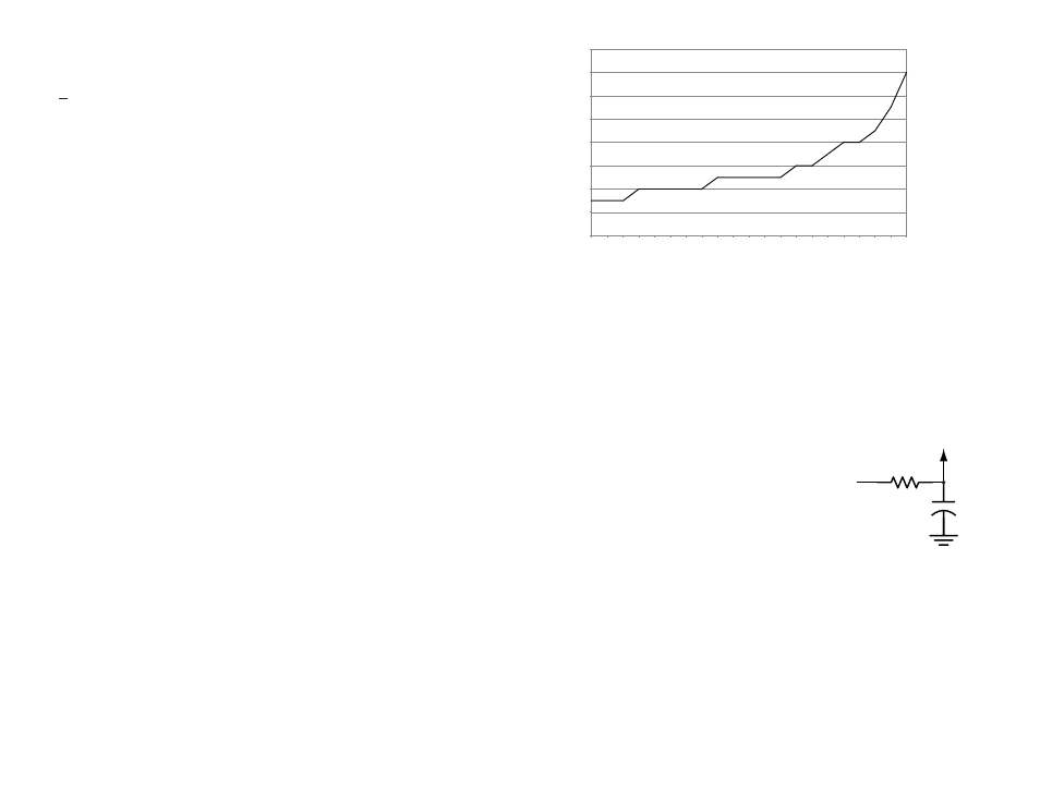
+
10
Ω
10
µF
Vcc IN
Vcc TO
MODULE
Figure 22: Supply Filter