4 test interface signals, Table 3.15 test interface signals, Test interface signals – Avago Technologies LSI53C876E User Manual
Page 91: Section 3.4, “test interface signals
Test Interface Signals
3-19
3.4 Test Interface Signals
describes the signals for the Test Interface Signals group.
MWE/
191, A7
O
4 mA
Memory Write Enable. This pin is used as a
write enable signal to an external Flash
memory.
MOE/_TESTOUT
192, B7
O
4 mA
Memory Output Enable. This pin is used as
an output enable signal to an external EPROM
or Flash memory during read operations. It is
also used to test the connectivity of the
LSI53C876E signals in the “AND-tree” test
mode. This pin is only driven as the Test Out
function when the TESTIN/ pin is driven LOW.
MCE/
193, A6
O
4 mA
Memory Chip Enable. This pin is used as a
chip enable signal to an external EPROM or
Flash memory device.
Table 3.14
ROM/Flash Interface Signals (Cont.)
Name
Pin No.
Type
Strength
Description
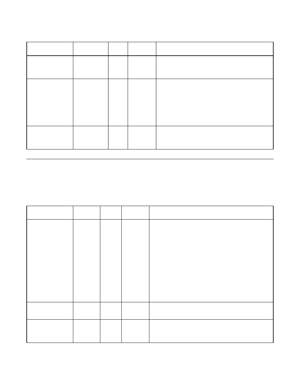
Table 3.15
Test Interface Signals
Name
Pin No.
Type
Strength
Description
TESTIN/
66, Y6
I
N/A
Test In. When this pin is driven LOW, the
LSI53C876E connects all inputs and outputs to an
“AND-tree”. The SCSI control signals and data
lines are not connected to the tree. The output of
the “AND-tree” is connected to the Test Out pin
(MOE/_TESTOUT). When the TESTIN/ pin is
driven LOW internal pull-ups are enabled on all
input, output, and bidirectional pins; all output and
bidirectional pins signals are 3-stated; and the
MOE/_TESTOUT pin is enabled. Connectivity is
tested by driving one of the LSI53C876E pins
LOW. The MOE/_TESTOUT should respond by
also driving LOW.
TCK
60, V5
I
N/A
Test Clock. This pin provides the clock for the
JTAG test logic. It has a static pull-up.
TMS
62, Y5
I
N/A
Test Mode Select. The signal received at TMS is
decoded by the TAP controller to control JTAG test
operations. It has a static pull-up.