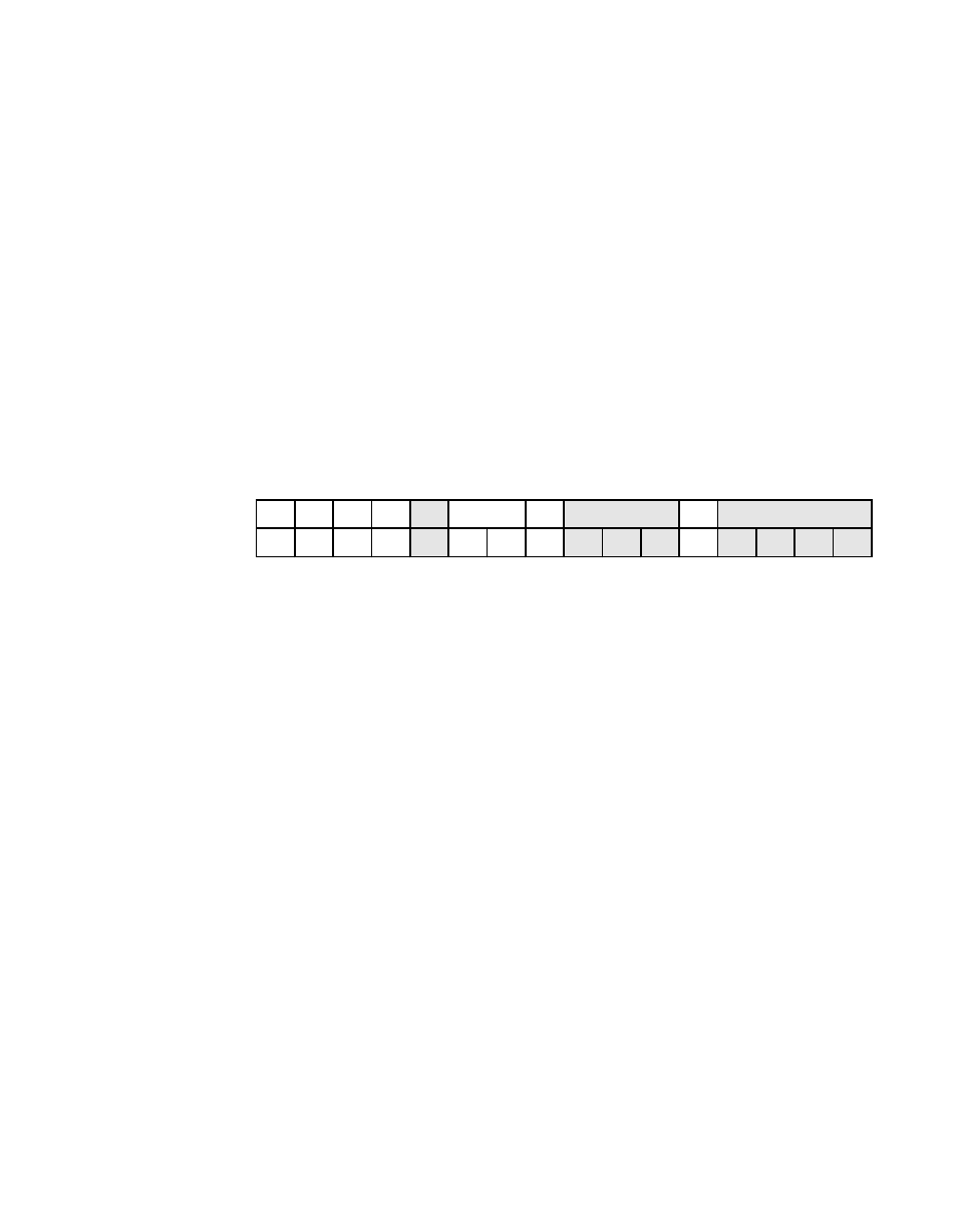
Status, Register: 0x06 – Avago Technologies LSI53C876E User Manual
Page 99

PCI Configuration Registers
4-5
registers in the SCSI function’s PCI
configuration space. In the LSI53C876E, this bit is
suppressed in Power State D2.
EIS
Enable I/O Space
0
This bit controls a SCSI function’s response to I/O space
accesses. A value of zero disables the device response.
A value of one allows the LSI53C876 to respond to I/O
Space accesses at the address range specified by the
Base Address Register Zero (I/O)
register in the SCSI
function’s PCI configuration space. In the LSI53C876E,
this bit is suppressed in Power State D2.
Register: 0x06
Status
Read/Write
Reads to this register behave normally. Writes are slightly different in that
bits can be cleared, but not set. A bit is cleared whenever the register is
written, and the data in the corresponding bit location is a one. For
instance, to clear bit 15 and not affect any other bits, write the value
0x8000 to the register.
DPE
Detected Parity Error (from Slave)
15
This bit is set by the a SCSI function of the LSI53C876
whenever it detects a data parity error, even if data parity
error handling is disabled.
SSE
Signaled System Error
14
This bit is set whenever the device asserts the SERR/
signal.
RMA
Received Master Abort (from Master)
13
A master device should set this bit whenever its
transaction (except for Special Cycle) is terminated with
Master Abort.
RTA
Received Target Abort (from Master)
12
A master device should set this bit whenever its
transaction is terminated by target abort.
15
14
13
12
11
10
9
8
7
5
4
3
0
DPE SSE RMA RTA
R
DT[1:0]
DPR
R
NC
R
0
0
0
0
0
0
0
0
0
0
0
1
0
0
0
0