Six states, Equivalent circuit – Fairchild SEMICONDUCTOR AN-7502 User Manual
Page 2
©2002 Fairchild Semiconductor Corporation
Application Note 7502 Rev. A1
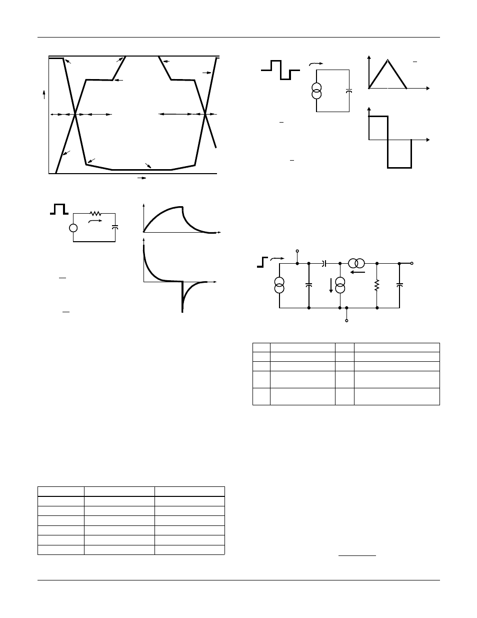
FIGURE 4.
IDEALIZED POWER MOSFET WAVEFORMS
FIGURE 5.
STEP-VOLTAGE FORCING FUNCTION
Power MOSFET devices are highly capacitive in nature;
hence, simple capacitor responses to the forcing functions
offer a good vehicle for comparison. The advantageous
choice is immediately obvious: Figure 6. Voltage/time
responses dominated by capacitance are straight lines
(when constant current is used). The slope of these lines is
proportional to current and inversely proportional to capaci-
tance. Analytically, then, constant current is most conve-
nient. It is quite another matter, however, to build a
bidirectional current drive that is accurate across the many
decades of both current and time required to establish
experimental verification.
Six States
To completely characterize power MOSFET switching wave-
forms, the six states that a device assumes, Figure 6, must
be addressed:
†
The term saturated is taken to mean a constant low-voltage drain-source
condition.
FIGURE 6.
STEP CURRENT FORCING FUNCTION
Equivalent Circuit
The lumped-parameter model of Figure 3, with the cascode-
connected JFET, can now be reduced to the linear equiva-
lent circuit of Figure 7, and the six device states investigated
from full off to full on.
FIGURE 7.
POWER MOSFET EQUIVALENT CIRCUIT
State 1: MOS Off, JFET Off
In a power-MOSFET device, no drain current will flow until
the device’s gate threshold voltage, V
gs(TH)
, is reached. Dur-
ing this time, the gate’s current drive is only charging the
gate source capacitance. More accurately, I
G
is charging
C
ISS
(C
ISS
= C
GS
+ C
GD
, C
DS
shorted), the capacitance
designation published by the industry.
The current generators, g
M
V
G
and g
MJ
V
X
are open circuits
for zero drain current, and R
L
is presumed to be so low as to
represent a short circuit (generally true for practical applica-
tions). This is academic however since C
GS
is very much
larger that C
X
. The time to reach threshold, then, is simply:
STATE
MOS
JFET
Turn-on 1
Off
Off
Turn-on 2
Active
Active
Turn-on 3
Active
Saturated
†
Turn-off 4
Saturated
Saturated
†
Turn-off 5
Active
Saturated
Turn-off 6
Active
Active
1
2
3
4
5
6
STATES
I
G
= CONSTANT
GATE VOLTAGE
DRAIN
VOLTAGE
V
G(SAT)
V
D(SAT)
V
DD
V
GS
VO
L
T
AG
E
V
T
V
DK
TIME
-V
G
i(
t)
v(
t)
t
t
-I
PK
= V
G
/R
O
I
PK
= V
G
/R
O
V
G
C
v(t)
i(t)
TURN ON
v(t) = V
G
(1 - e)
i(t) = V
G
e
R
O
TURN OFF
v(t) = V
G
e
i(t) = - V
G
e
R
O
-t/R
O
C
-t/R
O
C
-t/R
O
C
-t/R
O
C
R
O
LEGEND
V
GS
- Gate Voltage
C
DS
- Drain Source Capacitance
V
X
- JFET Driving Voltage
g
M
- MOSFET Transconductance
V
D
- Drain Voltage
g
MJ
- JFET Transconductance
C
GS
- Gate Source
Capacitance
R
L
- Drain Load Resistance
C
X
- MOSFET Feedback
Capacitance
I
G
- Constant Current Amplitude
T
1
=
C
ISS
V
gs(TH)
I
G
I
G
-I
G
i(t)
T
T
t
t
-I
G
I
G
i(
t)
v(t
)
v(t)
C
-VG =
C
I
G
T
TURN ON
v(t) =
I
G
t
C
i(t) = I
G
, 0 < t < T
TURN OFF
v(t) = 2V
G
-I
G
t
C
i(t) = I
G
, T < t < 2T
GATE
C
DS
SOURCE
DRAIN
C
X
V
GS
I
G
g
MJ
V
X
R
L
C
GS
g
M
V
G
V
D
V
X
Application Note 7502