Using the characterization curve, figure 9 – Fairchild SEMICONDUCTOR AN-7502 User Manual
Page 5
©2002 Fairchild Semiconductor Corporation
Application Note 7502 Rev. A1
Experimental Verification
Since the switching equations for step currents and voltages
differ only by gate-current magnitudes for the same device
type, one would expect a plot of switching time versus 1/R
O
to be of the same form as those obtained for a step current
drive. This is exactly the case, as Figure 10 is merely a vari-
ation of Figure 8. Using the relationships of Table 1, the
observed differences between Figures 7 and 9 can be pin-
pointed. The two sets of experimental curves confirm that,
on the basis of the short-circuit drive current V
G
/R
O
equal-
ling the constant I
G
, t
D
(on), t
R
, t
D
(off), and t
F
will all be
longer, as predicted by the ratios of the gate drive currents of
Table 1. Notice also that t
R
, t
F
switching symmetry is dis-
rupted by the use of a step voltage with source resistance
R
O
. For states 2 and 6 the time ratio is:
For states 3 and 5 the time ratio is:
Utilization of available maximum gate drive voltage and cur-
rent can be optimized for fastest power MOSFET switching
speed through the use of constant-current gate drive at the
expense of increased gate-drive circuit complexity.
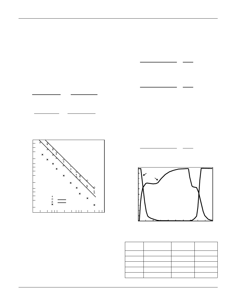
FIGURE 10.
CONSTANT GATE VOLTAGE SWITCHING TIME
Using the Characterization Curve,
Figure 9
To estimate the switching times for an RFM15N15 power
MOSFET under the conditions V
G
= 10V, V
DD
= 75V, R
O
=
100 ohms, and R
L
= 10 ohms, precedes as follows:
State 1: MOS Off, JFET Off
This time can be estimated without recourse to the curves
State 2 & 6: MOS Active, JFET Active
State 3: MOS Active, JFET Saturated
State 4: MOS Saturated, JFET Saturated
State 5: MOS Active, JFET Saturated
Figure 11 shows RFM15N15 waveforms using the conditions
specified in the example.
FIGURE 11.
STEP GATE VOLTAGE INPUT TO AN RFM15N15
t
TURN-ON
=
V
G(SAT)
t
TURN-OFF
V
G
- V
GS(TH)
t
TURN-ON
=
V
G(SAT)
t
TURN-OFF
V
G
- V
G(SAT)
10
1
0.1
0.01
10
-4
10
-3
10
-2
10
-1
DATA
t
D(OFF)
t
R
t
F
t
D(ON)
(t) -
M
IC
R
OS
E
C
ON
D
S
THEORY
1/R
O
RFM15N15
V
DD
= 75V
I
D
V
G
= 7.5A
= 10V
t =
100(1200 x 10
-12
) ln [1/(1 - 4/10)]
t =
61 ns
I
G
=
(10 - 4)/100 = 60mA
t =
(curve divisions) x I
T
µ
s
=
9
=
150ns
60
60
I
G
=
(10 - 7)/100 = 30mA
t =
(curve divisions) x I
T
µ
s
=
14
=
467ns
30
30
C
GS
+ C
x
=
(gate voltage slope)(test current)
=
(1.5 x 10
-6
s/5 volts)(10mA)
=
3000pF
t =
100(3000 x 10
-12
) ln [10/6.6]
t =
125ns
I
G
=
6.6/100 = 66mA
t =
(curve divisions) x I
T
µ
s
=
8
=
121ns
66
66
STATE
CALCULATED
TIME
MEASURED
TIME
RATIO
(t
C
, ns)
(t
M
, ns)
(t
C
/t
M
)
1
61
60
1.02
2 + 3
617
670
0.92
4
125
137
0.91
5 + 6
271
375
0.72
TIME - MICROSECONDS
DRAIN V
O
L
T
A
G
E
-
V
O
L
T
S
RFM15N15
V
DD
= 75 VOLTS
R
L
= 10 OHMS
V
G
= 10 VOLTS
R
O
= 100 OHMS
V
D
V
GS
0
75
0
1.5
3
Application Note 7502