A new device characterization – Fairchild SEMICONDUCTOR AN-7502 User Manual
Page 3
©2002 Fairchild Semiconductor Corporation
Application Note 7502 Rev. A1
State 2: MOS ActIve, JFET ActIve
This state graphically illustrates the dramatic influence that
the JFET has on the power MOSFET drain-voltage wave-
form. Instead of having to discharge C
x
from V
DD
to ground,
the lateral MOSFET need only swing V
X
to ground, a much
smaller voltage thanks to the grounded gate JFET. Since the
interaction of R
L
with the device capacitances has a second-
order effect on the drain voltage, the equivalent circuit of Fig-
ure 7 predicts a drain voltage change of:
dV
G
/dt = g
M
R
L
l
G
/[C
GS
+ C
X
(1 + g
M
/g
MJ
)]
In all but the smallest power-MOSFET devices, C
x
is several
thousand picofarads and g
M
/g
MJ
is of the order of 3:1.
Power-MOSFET devices exhibit a high dV
D
/dt switching rate
because of the cascode-connected JFET, not because
C
RSS
(C
RSS
= C
GD
) is a small value, as zero-drain-current
data sheet capacitance values might lead one to believe. If
C
RSS
were, in actuality, small, long drain voltage tails would
not exist. The tail response is a direct result of JFET satura-
tion. In order to delineate the transition from state 2 to state
3, a drain voltage at which the transition occurs must be
defined. V
DK
is the knee voltage at which linear extrapola-
tions of drain-voltage slopes intersect. The time duration of
state 2 is:
t
2
(t
6
) = (V
DD
- V
DK
)[C
GS
+ C
X
(1 + g
M
/g
M
J)]/g
M
R
L
I
G
State 3: MOS Active, JFET Saturated
When the JFET saturates, the g
MJ
V
X
current generator
becomes a short circuit and the equivalent circuit predicts:
dV
D
/dt = g
M
R
L
I
G
/[C
GS
+ C
X
(1 + g
M
R
L
)]
This is the Miller effect so often referred to in older texts that
describe the behavior of grounded-cathode vacuum-tube
amplifier circuits. Allowing for the fact that 1 + g
M
R
L
is
approximately equal to g
M
R
L
and C
X
(1 + g
M
R
L
) is very
much larger than C
GS
, the expression for drain-voltage tail
time is:
t
3
(t
5
) = (V
DK
- V
D(SAT)
)C
x
/l
G
State 4: MOS Saturated, JFET Saturated (Turn-Off)
In this state, in addition to g
MJ
V
X
being shorted, the g
M
V
G
cur-
rent generator is shorted, and I
G
is occupied with charging C
X
and C
GS
, in parallel, from the peak value of V
G
to V
G(SAT)
. The
time required for this is:
t
4
= (V
G
- V
G(SAT)
)(C
GS
+ C
x
)/I
G
Since a value for C
GS
may be measured independently of
switching time, the method described is the simplest way of
determining C
X
.
On turn-off, the state time equations are equally applicable,
but in reverse order (states 5 and 6); see the idealized wave-
form of Figure 4.
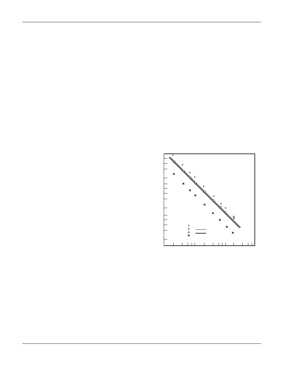
Experimental Verification
The four switching states just analyzed indicate that for a
given device, all four switching state times are inversely pro-
portional to the magnitude of the gate drive current. Figure 8
illustrates the switching performance of a typical power
MOSFET across three decades of gate drive current and
time. In each case the data slope is almost a perfect -1.
A New Device Characterization
Figure 8 could not be a reasonable device data sheet pre-
sentation because it does not give the designer any informa-
tion on a typical value for C
X
, nor does it convey how V
DK
,
g
M
, g
M
/g
MJ
, and V
G
(sat) vary with drain current. What would
be of enormous value to the designer is a plot of V
D
(t), V
G
(t)
for selected values of V
DD
and I
D
within device ratings.
A reasonable characterization would be as follows:
1. The x axis would be normalized in terms of gate current drive.
2. The y axis would be normalized in terms of percent maximum rated
BV
DSS
(0 to 100%).
3. R
L
= BV
DSS
/I
D(max)
would define the drain load resistance.
4. Four plots of V
D
(t), V
G
(t) at 100%, 75%, 50%, and 25% BV
DSS(max)
would be shown.
FIGURE 8.
CONSTANT GATE CURRENT SWITCHING TIME
Figure 9 is such a plot for the RFM15N15 power MOSFET.
With such a plot, a designer can estimate device switching
performance under any resistive gate/drain conditions.
10
1
0.1
0.01
1
10
100
1000
RFM15N15
V
DD
= 75V
I
D
R
O
V
G
= 7.5A
=
∞
Ω
= 10V
(t
) -
MI
C
R
OS
E
C
ON
D
S
(I
G
) - MILLIAMPERES
DATA
t
D(OFF)
t
R
t
F
t
D(ON)
THEORY
Application Note 7502