Step-voltage gate drive – Fairchild SEMICONDUCTOR AN-7502 User Manual
Page 4
©2002 Fairchild Semiconductor Corporation
Application Note 7502 Rev. A1
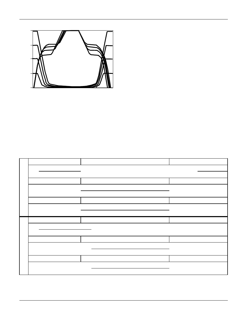
FIGURE 9. NORMALIZED RFM15N15 SWITCHING WAVE-
FORMS FOR CANSTANT GATE-CURRENT DRIVE.
Step-Voltage Gate Drive
The majority of power MOSFET applications employ a step
gate-voltage input with a finite source resistance R
O
. Often
R
O
for turn-on is not the same as R
O
for turn-off. How can
switching times for these situations be estimated using the
switching characterization curves just described? The analy-
sis for resistive step voltage inputs, which is complex
because the gate current is no longer constrained to be con-
stant, but is a function of device gate-voltage response, is
covered in Appendix A. (A second, shorter appendix, B, has
been added to illustrate the estimation of R
O
for some practi-
cal gate drive circuits.) Table 1 summarizes the common
switching equations, and indicates the appropriate 1
G
to be
used in each state for relating step voltage drives to the char-
acterization curves.
Experimental Verification
Since the switching equations for step currents and voltages
differ only by gate-current magnitudes for the same device
type, one would expect a plot of switching time versus 1/R
O
to be of the same form as those obtained for a step current
drive. This is exactly the case, as Figure 10 is merely a vari-
ation of Figure 8. Using the relationships of Table 1, the
observed differences between Figures 7 and 9 can be pin-
pointed. The two sets of experimental curves confirm that,
on the basis of the short-circuit drive current V
G
/R
O
equal-
ling the constant I
G
, t
D(on)
, t
R
, t
D(off)
, and t
F
will all be
longer, as predicted by the ratios of the gate drive currents of
Table 1. Notice also that t
R
, t
F
switching symmetry is dis-
rupted by the use of a step voltage with source resistance
R
O
. For states 2 and 6 the time ratio is:
100
75
50
25
0
20I
T
/I
G
40I
T
/I
G
60I
T
/I
G
80I
T
/I
G
RFM15N15
I
T
= 1mA
V
G
= 10 VOLTS
R
L
= V
DSS
/I
D(RMS)
% RA
T
ES V
DSS
TIME - microseconds
TABLE 1.
COMMON SWITCHING EQUATIONS
T
U
R
N
O
N
CONSTANT CURRENT
STATE 1: MOS OFF, JFET OFF
CONSTANT VOLTAGE
t =
C
ISS
V
GS(TH)
t = R
O
C
ISS
In
[1]
I
G
[1 - V
GS(TH)
/V
G
]
I
G
= I
T
STATE 2: ACTIVE, ACTIVE
I
G
= (V
G
- V
GS(TH)
)/R
O
t =
[V
DD
- V
DK
] [C
GS
+ C
x
(1 + g
M
/g
MJ
)]
g
M
R
L
I
G
I
G
= I
T
STATE 3: ACTIVE, SATURATED
I
G
= (V
G
- V
G(SAT)
)/R
O
t =
(V
DK
- V
D(SAT)
)C
X
I
G
T
U
R
N
O
F
F
I
G
= I
T
STATE 4: SATURATED, SATURATED
I
G
= -V
G
/R
O
t =
(C
GS
+ C
X
)(V
G
- V
G(SAT)
)
t = R
O
(C
GS
+ C
X
) In (V
G
/V
G(SAT)
)
I
G
I
G
= I
T
STATE 5: ACTIVE, SATURATED
I
G
= (V
G
- V
G(SAT)
)/R
O
t =
(V
DK
- V
D(SAT)
)C
X
I
G
I
G
= I
T
STATE 6: ACTIVE, ACTIVE
I
G
= (V
G
- V
G(SAT)
)/R
O
t =
[V
DD
- V
DK
] [C
GS
+ C
X
(1 + g
M
/g
MJ
)]
g
M
R
L
I
G
Application Note 7502